Packaging structure and packaging method of high-pixel image sensing chip

An image sensor chip and packaging structure technology, applied in radiation control devices, electrical components, electric solid state devices, etc., can solve the problem of unfavorable image sensor chip stress release, complex process reliability and stability, and easy generation of ghost images. or glare and other problems, to achieve the effect of improving reliability and stability, fewer production process steps, and saving economic costs

Active Publication Date: 2016-02-24
HUATIAN TECH KUNSHAN ELECTRONICS
View PDF4 Cites 5 Cited by
  • Summary
  • Abstract
  • Description
  • Claims
  • Application Information

AI Technical Summary

Problems solved by technology

[0002] The packaging of high-pixel image sensor chips requires a large gap between the sensing area and the light-transmitting substrate, otherwise the particles on the light-transmitting substrate will have a greater impact on the sensing area, and ghost images or glare are likely to occur and other adverse phenomena; a packaging process is to expose the pads of the image sensor chip on the surface of the substrate by using a through-silicon hole process, and lay an insulating layer, a metal circuit layer, and a protective layer on the surface of the substrate to connect the contacts on the chip to the wires. On the internal pins of the frame, and then transmit the circuit signal of the chip to the external circuit board, the production cost is high, the process is complicated, and it is not conducive to the release of the internal stress of the image sensor chip
Another packaging process is to use COB packaging technology to directly mount the image sensor chip on the circuit board by using adhesives or automatic tape welding, wire bonding, flip-chip welding, etc., and then realize the image sensor through wire bonding technology. The solder pads on the chip are electrically connected to the connection points on the circuit board. Although the performance of the packaged product is reliable and stable, the packaged product is small in size and the cost of the package is low, the sensing area of ​​the image sensor chip is in the COB package. It is easy to be polluted or damaged during the process, and it is necessary to protect the sensing area of ​​the image sensor chip. At the same time, complex process steps are required (for example, firstly use a cutting process to remove most of the protective material, and then use an etching process to remove most of the protective material, and then use an etching process to remove protective material) to expose the pads of the image sensor chip for wire bonding. Similarly, there are technical problems such as complex process, reliability and stability.

Method used


Image

  • Packaging structure and packaging method of high-pixel image sensing chip
  • Packaging structure and packaging method of high-pixel image sensing chip
  • Packaging structure and packaging method of high-pixel image sensing chip

Examples


Embodiment Construction

[0038] In order to understand the technical content of the present invention more clearly, the following examples are given in detail, the purpose of which is only to better understand the content of the present invention but not to limit the protection scope of the present invention. For convenience of description, the components in the structures in the drawings of the embodiments are not scaled according to the normal scale, so they do not represent the actual relative sizes of the structures in the embodiments.

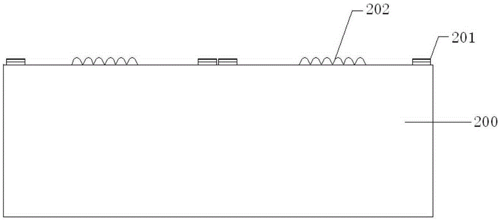
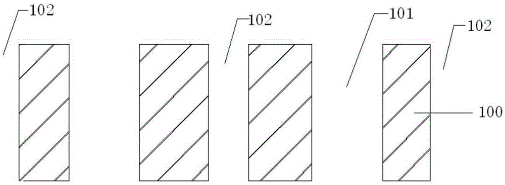
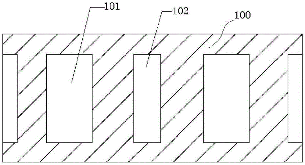
[0039] Such as Figure 9 As shown, a packaging structure of a high-pixel image sensor chip includes a carrier unit 100, an image sensor chip 200, a light-transmitting substrate 300, and a functional substrate 500. The functional surface of the image sensor chip has a sensing area 202 and several welding pads 201 located around the sensing area, the carrier unit is formed with a first cavity 101 and at least one second cavity 102 passing through its upper and lower...


PUM


Abstract

The invention discloses a packaging structure and packaging method of a high-pixel image sensing chip. A first through hollow cavity is manufactured in a carrier board, a second through hollow cavity is manufactured at the same time, the carrier board and the first hollow cavity in the carrier board can provide a large gap for a sensing region of the high-pixel image sensing chip and a light-transmission substrate, a role in protecting the sensing region from being polluted or damaged is played in the packaging process, and packaging reliability and stability are improved. Welding pads of the image sensing chip are exposed through the second hollow cavity, the electric property of the image sensing chip can be leaded out to a functional substrate through direct routing; compared with the traditional silicon through hole process, the packaging method does not need to lay an insulation layer, a metal circuit layer and the like but directly leads out the electric property, has the advantages of the simple manufacture procedure and the small volume of a packaging body, and can effectively save economic cost at the same time; and the first through hollow cavity is manufactured in the carrier board, the second through hollow cavity is manufactured at the same time, so the manufacturing process steps are reduced, and the process is very simple.

Description

technical field [0001] The invention relates to the packaging of an image sensor chip, in particular to a packaging structure and a packaging method of a high-pixel image sensor chip. Background technique [0002] The packaging of high-pixel image sensor chips requires a large gap between the sensing area and the light-transmitting substrate, otherwise the particles on the light-transmitting substrate will have a greater impact on the sensing area, and ghost images or glare are likely to occur and other adverse phenomena; a packaging process is to expose the pads of the image sensor chip on the surface of the substrate by using the through-silicon hole process, and lay an insulating layer, a metal circuit layer, and a protective layer on the surface of the substrate to connect the contacts on the chip to the wires. The internal pins on the frame transmit the circuit signals of the chip to the external circuit board, which is costly and complicated to manufacture, and is not ...

Claims


Application Information

Patent Timeline
Patent Type & Authority Applications(China)
IPC IPC(8): H01L27/146H01L21/56H01L21/60
CPCH01L21/56H01L24/64H01L27/14601
Inventor 万里兮马力钱静娴陈仁章豆菲菲翟玲玲
Owner HUATIAN TECH KUNSHAN ELECTRONICS
Why Eureka
Try Eureka