LED chip and manufacturing method

A technology of LED chip and manufacturing method, which is applied in the direction of electrical components, circuits, semiconductor devices, etc., can solve the problems of reducing product yield, increasing chip voltage, reducing chip light emission, etc., so as to improve yield and prevent desoldering and fragmentation , the effect of reducing damage

Active Publication Date: 2016-02-24
FOSHAN NATIONSTAR SEMICON
View PDF14 Cites 5 Cited by
  • Summary
  • Abstract
  • Description
  • Claims
  • Application Information

AI Technical Summary

Problems solved by technology

[0002] At present, most of the LED chips use sapphire as the substrate, and the sapphire substrate is thick, so the heat is difficult to export, and the heat gathers on the chip to affect the reliability of the chip, increase the light decay and reduce the life of the chip; 2) due to the electrode block 3) Current crowding will increase the voltage of the chip, which will reduce the luminous efficiency of the chip; 4) The packaging is complicated, and the voltage of a single LED chip is about 3V, so it needs Transforming voltage or packaging them in series, these increase the difficulty of packaging and application, the process difficulty increases, and the reliability of the entire chip deteriorates
[0003] In the prior art, the sapphire substrate is generally peeled off by laser, but when the laser is peeled off the sapphire substrate, the laser is absorbed by the gallium nitride at the interface between the sapphire and the epitaxial layer, and the local temperature of the gallium nitride reaches more than 900°C, making the nitride Gallium thermally decomposes, generating a large amount of heat, uneven heat release, and heat accumulation in local areas, which is likely to cause damage to the chip and affect the photoelectric performance of the chip. In addition, the use of laser to peel off the substrate may easily lead to chip fragmentation, desoldering, etc., reducing product quality. Rate

Method used


Image

  • LED chip and manufacturing method
  • LED chip and manufacturing method
  • LED chip and manufacturing method

Examples


Embodiment Construction

[0042] The technical solutions in the embodiments of the present invention will be clearly and completely described below in conjunction with the accompanying drawings in the embodiments of the present invention. Obviously, the described embodiments are only a part of the embodiments of the present invention, rather than all the embodiments. Based on the embodiments of the present invention, all other embodiments obtained by those of ordinary skill in the art without creative work shall fall within the protection scope of the present invention.

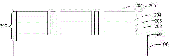
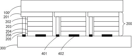
[0043] Combine Figure 1 to Figure 2g As shown, figure 1 A flow chart of a method for manufacturing an LED chip provided by an embodiment of this application, Figure 2a to Figure 2g for figure 1 The structure flow chart corresponding to the production method flow chart; where the production method includes:

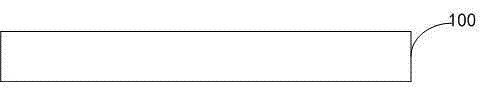
[0044] S1. Provide a sapphire substrate.

[0045] reference Figure 2a As shown, a sapphire substrate 100 is provided.

[0046] S2. Fa...


PUM


Abstract

The invention discloses an LED chip and a manufacturing method. The manufacturing method comprises steps of fixing substrates on sides of N type electrodes and P type electrodes of a plurality of luminescence microstructures, wherein the sides of the N type electrodes and the P type electrodes are away from a sapphire substrate, thinning and cutting a sapphire substrate, filling a gap between the luminescence microstructure and the substrate, strippingthe substrate by the laser, and cutting the substrate into independent LED chips, which enables the luminescence microstructure to be fully fixed on the substrate. The invention effectively prevents the light emitting microstructure from unsoldering and fragmentation.

Description

Technical field [0001] The invention relates to the technical field of light emitting diodes, and more specifically, to an LED chip and a manufacturing method thereof. Background technique [0002] At present, most of the LED chips use sapphire as the substrate, and the sapphire substrate is thicker, so it is difficult to dissipate heat. The heat accumulation on the chip affects the reliability of the chip, increases light attenuation and reduces chip life; 2) due to electrode blocking Light will reduce the light output of the chip, leading to the problem of low light efficiency; 3) Current crowding will increase the voltage of the chip, which will reduce the light efficiency of the chip; 4) The package is complicated, and the voltage of a single LED chip is about 3V, so it needs Transformation or packaging to connect them in series increases the difficulty of packaging and application, and the difficulty of the process increases, which makes the reliability of the entire chip wo...

Claims


Application Information

Patent Timeline
Patent Type & Authority Applications(China)
IPC IPC(8): H01L33/00H01L33/64H01L33/52
CPCH01L33/005H01L33/52H01L33/64H01L33/642
Inventor 徐亮何键云
Owner FOSHAN NATIONSTAR SEMICON
Why Eureka
Try Eureka