A device for vapor deposition of thin films

A vapor deposition and thin film technology, which is applied in the direction of gaseous chemical plating, metal material coating process, coating, etc., can solve the problems of unfavorable deposition of thin film, thermal deformation, and inability to ensure temperature uniformity, so as to ensure uniformity, Effect of extended service life and good temperature uniformity

Active Publication Date: 2018-06-19
HUAZHONG UNIV OF SCI & TECH
View PDF5 Cites 0 Cited by
  • Summary
  • Abstract
  • Description
  • Claims
  • Application Information

AI Technical Summary

Problems solved by technology

However, usually due to the reaction chamber design, or the installation of the heater, good temperature uniformity cannot be guaranteed
At the same time, due to the introduction of the heating device, the temperature in the local area of ​​the heater may be higher than other positions, which will easily lead to thermal deformation
These are not conducive to depositing good films

Method used


Image

  • A device for vapor deposition of thin films
  • A device for vapor deposition of thin films
  • A device for vapor deposition of thin films

Examples


Embodiment 1

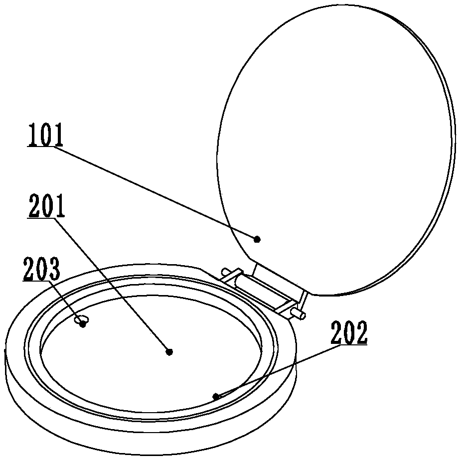
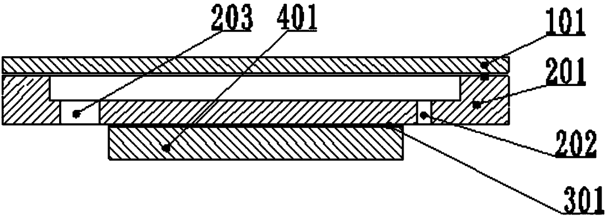
[0035] In actual use of the equipment, the heating temperature usually reaches 200°C. After a period of heating, the inner surface of the cavity warps, and the central area of ​​the disc is 2-3mm higher than the surrounding area. When the silicon wafer is put into the cavity, the silicon wafer cannot be well bonded to the inner surface of the cavity, and the contact only occurs in a local area. Due to the warpage of the inner surface of the cavity, the temperature distribution on the silicon wafer is inconsistent, which also leads to the inconsistent deposition of thin films on the silicon wafer. In order to ensure uniform deposition on the silicon wafer, the design of the cavity is improved by adding a ring groove to avoid warping and deformation of the cavity.

[0036] The effect of this anti-deformation groove can be verified by simulation. It can be seen from the temperature simulation that after adding the annular groove, the temperature on the inner surface of the cavit...

Embodiment 2

[0038] Apply the vapor phase film deposition device provided by the present invention to deposit an ALD aluminum oxide film with a thickness of 20 nm on the surface of a silicon wafer.

[0039] Two kinds of reactants are used in the embodiment, the reactant A is trimethylaluminum, and the reactant B is water. Nitrogen is used as the carrier gas of the reactants, and the flow rate of the carrier gas is 100 sccm.

[0040] The reaction temperature was set at 180°C, and a 4-inch silicon wafer was used as the substrate for the reaction. Put the cleaned silicon wafer into the chamber and vacuumize the chamber. When the pressure in the cavity is pumped below 10Pa, start heating, and the temperature of the cavity will rise rapidly. When the temperature in the cavity is stabilized at 180±3°C, open the valve of the reactant A trimethylaluminum for 1 second, at this time the reactant A trimethylaluminum enters the cavity in the form of pulses. After the reactant A, trimethylaluminum, ...


PUM

PropertyMeasurementUnit
widthaaaaaaaaaa
depthaaaaaaaaaa
thicknessaaaaaaaaaa

Abstract

The invention discloses a device for vapor deposition of thin films, which comprises a reaction chamber upper cover, a reaction chamber base and a heater; the reaction chamber base is used to carry a substrate, and is movably linked with the reaction chamber upper cover A vapor deposition reaction chamber is formed, the back of which is in contact with the heater for heat conduction; the base of the reaction chamber is circular and has an annular groove. The device provided by the invention is used for vapor phase deposition of thin films, which can ensure that the overall reaction chamber will not be deformed too much, thereby ensuring the uniformity of the thin film.

Description

technical field [0001] The invention belongs to the field of vapor phase reaction deposition film, and more specifically relates to a device for vapor phase deposition film. Background technique [0002] With the rapid development of semiconductor technology, higher requirements are put forward for semiconductor equipment. Thin film deposition technology is one of the very important supporting technologies in the semiconductor field. [0003] In the field of semiconductor manufacturing, it is usually necessary to fabricate numerous microstructures on a substrate. These structures with special functions are basically at the micro-nano scale. To form such a tiny structure, traditional processing methods cannot be completed. Depositing a thin film on a substrate is an important method to complete this microscopic processing. [0004] Vapor deposition is a thin film deposition technique widely used in industrial applications, and it can be used to deposit most insulating and...

Claims


Application Information

Patent Timeline
Patent Type & Authority Patents(China)
IPC IPC(8): C23C16/44
Inventor 陈蓉林骥龙何文杰王晓雷马玉春但威单斌
Owner HUAZHONG UNIV OF SCI & TECH
Why Eureka
Try Eureka