Semiconductor device, manufacturing method therefor, and electronic device

A technology for electronic devices and semiconductors, applied in the fields of semiconductor devices, semiconductor/solid-state device manufacturing, and electrical solid-state devices, etc., can solve the problems of increasing the number of steps, increasing product costs, affecting shipments, etc., to increase shipments, The effect of reducing process cost and reducing the risk of leakage

Inactive Publication Date: 2016-03-09
SEMICON MFG INT (SHANGHAI) CORP
View PDF7 Cites 2 Cited by
  • Summary
  • Abstract
  • Description
  • Claims
  • Application Information

AI Technical Summary

Problems solved by technology

But described method has not only increased the number of the step of technology, has improved product cost, and has reduced output (Throughput), has influenced shipments

Method used


Image

  • Semiconductor device, manufacturing method therefor, and electronic device
  • Semiconductor device, manufacturing method therefor, and electronic device
  • Semiconductor device, manufacturing method therefor, and electronic device

Examples


preparation example Construction

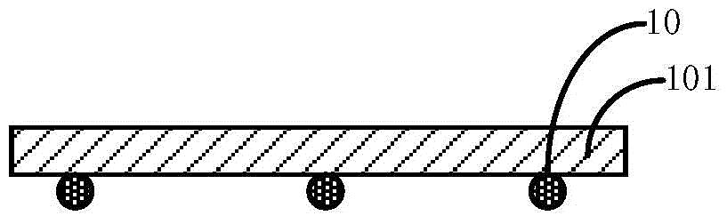
[0048] Current methods of fabricating semiconductor devices such as Figures 1a-1d As shown, wherein, a first wafer 101 is provided first, and a bump generation process (Bump) is performed to form several bonding bumps 10 on the first wafer 101, as Figure 1a shown.

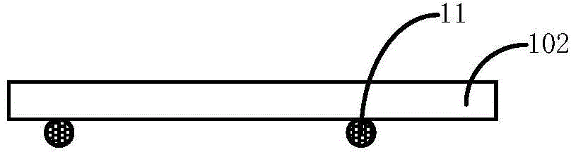
[0049] Then a second wafer 102 is provided, and a bump generation process (Bump) is also performed to form several bonding bumps 11 on the second wafer 102, such as Figure 1bshown.

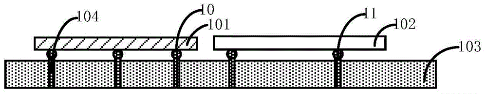
[0050] A third wafer 103 is provided, wherein a number of through-silicon vias 104 (TSVs) are formed in the third wafer 103 for realizing connections, such as Figure 1c shown.

[0051] Alternatively, the third wafer 103 is selected as an interposer, and the first wafer 101, the second wafer 102, and the third wafer 103 are connected together through a flip-chip bump process (Bump) for signal transmission. Such as Figure 1d shown. However, the method not only increases the number of steps in the process and increases the cost ...

Embodiment 1

[0054] In order to solve the problems in the prior art, the present invention provides a method for preparing a semiconductor device, the following in conjunction with the attached Figure 2a-2f The method is described further.

[0055] First, step 201 is performed to provide a bottom wafer 201 .

[0056] Specifically, such as Figure 2a As shown, the bottom wafer 201 may be a memory wafer, for example, various memory devices or units may be formed on the bottom wafer.

[0057] Optionally, other active or passive devices may also be formed in the bottom wafer, and are not limited to a certain one, which will not be repeated here.

[0058] Step 202 is executed to form an insulating layer 202 on the bottom wafer 201 .

[0059] Specifically, such as Figure 2b As shown, in this step, an insulating layer 202 is formed on the bottom wafer 201 to completely cover the bottom wafer 201. Optionally, the insulating layer 202 is made of an organic insulating material, which can not o...

Embodiment 2

[0091] The present invention also provides a semiconductor device, comprising:

[0092] bottom wafer 201;

[0093] an insulating layer 202 located above the bottom wafer;

[0094] interconnection vias 20 located in the insulating layer and connected to the bottom wafer;

[0095] The top wafer 203 is located above the insulating layer, wherein bumps 204 are formed on the top wafer, and the bumps are connected to the interconnection vias.

[0096] Wherein, the bottom wafer 201 may be a storage wafer, for example, various storage devices or units may be formed on the bottom wafer. Optionally, various active or passive devices may also be formed on the bottom wafer, and are not limited to a certain one, which will not be repeated here.

[0097] The insulating layer 202 is made of an organic insulating material, which not only reduces the risk of electric leakage, but also improves the breakdown resistance. Optionally, the insulating layer 202 may be polyimide.

[0098] In the...


PUM


Abstract

The invention relates to a semiconductor device, a manufacturing method therefor, and an electronic device. The method comprises the steps: S1, providing a bottom wafer; S2, forming an insulating layer on the bottom wafer, and forming a plurality of interconnection through holes in the insulating layer, so as to connect the bottom wafer; S3, providing a top wafer, and forming a plurality of convex points, matched with the interconnection through holes, on the top wafer; S4, enabling the interconnection through holes to be connected with the convex points, so as to form a flip chip. The method is advantageous in that (1) the method reduces the technology of one-time Bump, and reduces the technological cost; (2) the method reduces one wafer serving as an interlayer (Interposer) and the interlayer technology, and increases the output; (3) the method takes organic matters as insulating materials, reduces the risks of electric leakage, and improves the capability of breakdown resistance.

Description

technical field [0001] The present invention relates to the field of semiconductors, in particular, the present invention relates to a semiconductor device, a preparation method thereof, and an electronic device. Background technique [0002] In the field of electronic consumption, multi-function devices are more and more popular among consumers. Compared with devices with simple functions, the production process of multi-function devices will be more complicated, such as the need to integrate multiple chips with different functions on the circuit board, so 3D integrated circuit (integrated circuit, IC) technology, 3D integrated circuit (integrated circuit, IC) is defined as a system-level integrated structure, stacking multiple chips in the vertical plane direction, thereby saving space, the edge of each chip can be according to It is necessary to lead out multiple pins, and use these pins to interconnect the chips that need to be connected to each other through metal wires...

Claims


Application Information

Patent Timeline
IPC IPC(8): H01L21/768H01L21/60H01L25/065
Inventor 郑超王伟
Owner SEMICON MFG INT (SHANGHAI) CORP
Why Eureka
Try Eureka