Epitaxial wafer for triode and preparation method thereof

A technology of epitaxial wafers and triodes, applied in semiconductor/solid-state device manufacturing, electrical components, circuits, etc., can solve problems such as easy breakdown, high dislocation density, high leakage current of triode electronic devices, and achieve high breakdown voltage , good crystal quality and low leakage current

Inactive Publication Date: 2016-03-16
JIANGSU CORENERGY SEMICON CO LTD
View PDF3 Cites 0 Cited by
  • Summary
  • Abstract
  • Description
  • Claims
  • Application Information

AI Technical Summary

Problems solved by technology

Due to the high dislocation density of the flat sapphire substrate commonly used in the prior ar

Method used


Image

  • Epitaxial wafer for triode and preparation method thereof

Examples


Embodiment Construction

[0026] Preferred embodiments of the present invention are described in detail below, so that the advantages and features of the present invention can be more easily understood by those skilled in the art.

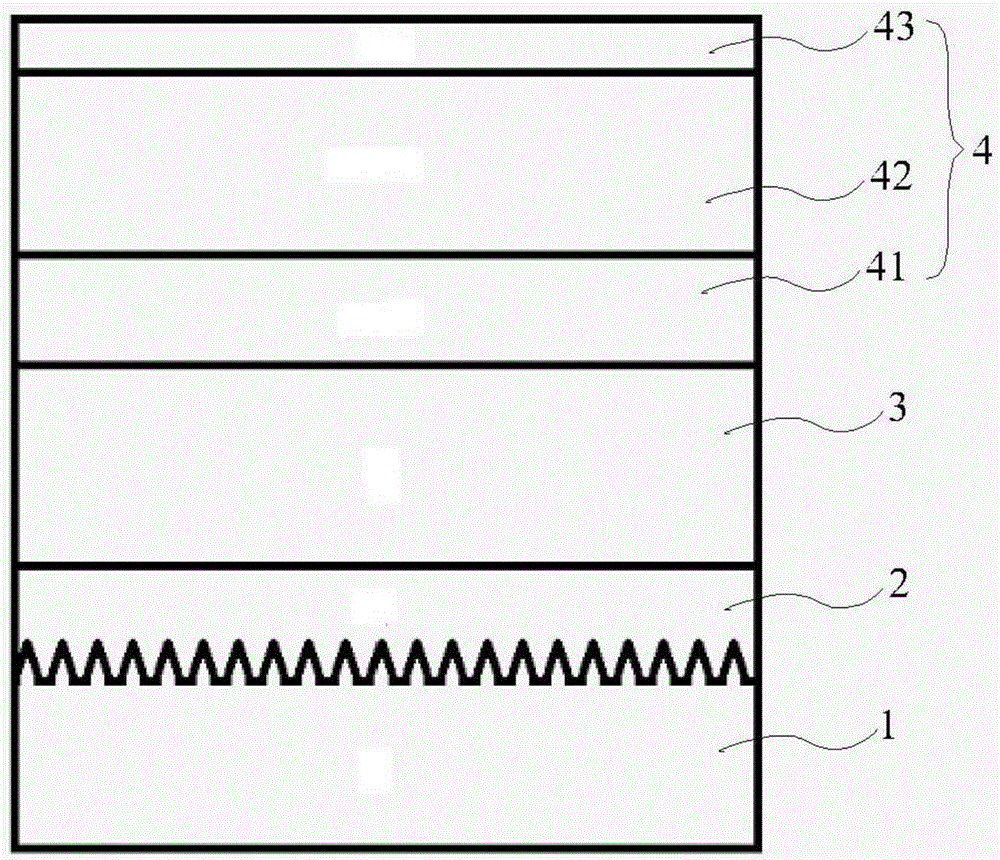
[0027] figure 1 Shown is an epitaxial wafer for a tertiary tube of the present invention. combine figure 1 As shown, the triode epitaxial wafer includes a substrate 1 , a GaN nucleation layer 2 , a GaN buffer layer 3 , a GaN channel layer 41 , an InAlN intrinsic layer 42 , and a GaN capping layer 43 stacked in sequence.

[0028] The substrate 1 is a patterned sapphire substrate (PSS) 1 . The pattern height, width, and gap of the patterned sapphire substrate 1 are 1.6 μm, 2.4 μm, and 0.6 μm respectively; or, the pattern height, width, and gap of the patterned sapphire substrate 1 are 1.7 μm, 2.6 μm, and 0.4 μm, respectively; Or, the pattern height, width, and gap of the patterned sapphire substrate 1 are 1.2 μm, 1.8 μm, and 0.1 μm, respectively.

[0029] The n...


PUM

PropertyMeasurementUnit
Thicknessaaaaaaaaaa
Thicknessaaaaaaaaaa
Thicknessaaaaaaaaaa

Abstract

The invention provides an epitaxial wafer for a triode and a preparation method thereof. A triode electronic device prepared by the epitaxial wafer has the advantages of low electric leakage, a high breakdown voltage and the long service life. The epitaxial wafer for the triode comprises a substrate, a GaN nucleation layer, a GaN buffer layer, a GaN channel layer and an InAlN intrinsic layer and a GaN cover layer which are successively stacked; and the substrate is a graphical sapphire substrate, the GaN nucleation layer is a C-doped GaN nucleation layer, and the GaN buffer layer is a C-doped GaN buffer layer.

Description

technical field [0001] The invention relates to an epitaxial wafer for a triode and a preparation method thereof, in particular to an epitaxial wafer for a triode using an imaged sapphire substrate and a preparation method thereof. Background technique [0002] There are two main types of substrates currently used for epitaxial wafers of triodes, namely sapphire substrates and silicon carbide substrates. However, due to the high price of silicon carbide, sapphire substrates are more widely used. Due to the high dislocation density of the flat sapphire substrate commonly used in the prior art, the triode electronic device made of it has high leakage current and is easy to break down. Contents of the invention [0003] In view of the above problems, the object of the present invention is to provide an epitaxial wafer for a triode and its preparation method, the triode electronic device made of it has low leakage, high breakdown voltage and long service life. [0004] In or...

Claims


Application Information

Patent Timeline
IPC IPC(8): H01L29/20H01L21/02
CPCH01L29/2003H01L21/0254H01L21/0262
Inventor 王东盛苗操李亦衡魏鸿源严文胜张葶葶朱廷刚
Owner JIANGSU CORENERGY SEMICON CO LTD
Why Eureka
Try Eureka