

Method for preparing InN film material by taking In2O3 as target material
A thin film material and target material technology, which is applied in the field of nitride photoelectric thin film material preparation, can solve the problems of InN thin film XRD diffraction peak intensity, substrate miscellaneous peaks, uneven growth, etc., and achieve microscopic morphology with large particles and crystallization Good quality and uniform effect
- Summary
- Abstract
- Description
- Claims
- Application Information
AI Technical Summary
Problems solved by technology
Method used
Image

Examples
Embodiment 1
[0041] This embodiment provides a 2 o 3 The method for preparing the InN thin film material for the target material, the steps are as follows,
[0042] Step 1, place the cut unpolished 1cm×1cm silicon wafer Si(100) substrate in a 100ml beaker, pour a solution of acetone solution and carbon tetrachloride with a volume ratio of 1:1 into the beaker, Until the mixed solution submerges the silicon wafer, in order to prevent external environmental pollution during cleaning, seal the beaker with clean dust-free paper; place the beaker in an ultrasonic cleaner, set the cleaning time to 30 minutes, and repeat twice; Wash the silicon wafer with water and ethanol for 30 minutes, repeat twice; wash the silicon wafer with deionized water for 30 minutes, repeat twice to get a clean silicon wafer, and finally place the cleaned silicon wafer in the container Store in glass vials of absolute ethanol for subsequent use.
[0043] Step 2, place the washed silicon wafer Si (100) on the circular...
Embodiment 2
[0055] This embodiment provides a method for preparing a thin film material. The preparation steps are the same as those in Embodiment 1, except that the chamber temperature is 600°C.
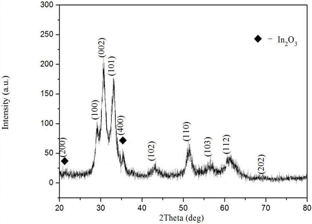
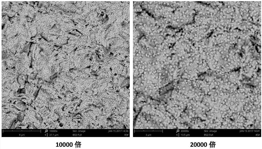
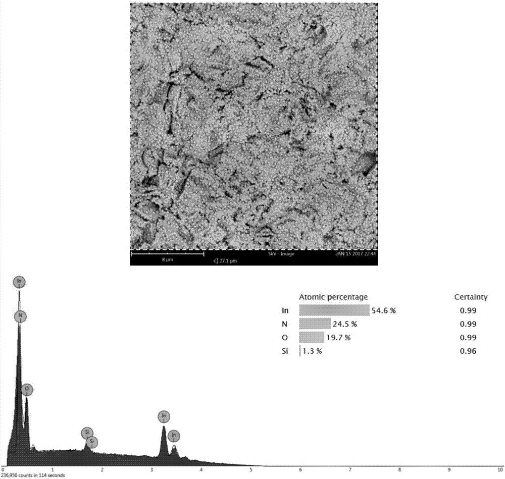
[0056] pass Figure 10 According to the XRD analysis, the sample at the sputtering temperature of 600°C is a high-purity InN thin film material, which is passed Figure 11 SEM and Figure 12 The EDS analysis further confirmed that it is a pure InN thin film material, and the average grain size is 650nm, the grain size is uniform, and there are no miscellaneous peaks.
Embodiment 3
[0061] This embodiment provides a method for preparing a thin film material, the preparation steps are the same as in Embodiment 1, the difference is that the sputtering pressure is 1.2Pa
[0062] pass Figure 16 According to the XRD analysis, the sample under the sputtering pressure of 1.2Pa is an InN thin film material, and the diffraction peak of the substrate Si appears. Figure 17 SEM and Figure 18 According to the EDS analysis, the Si element content is relatively high, and the obtained InN thin film material is not very good in crystallinity.
PUM
| Property | Measurement | Unit |
|---|---|---|
| Average size | aaaaa | aaaaa |
Abstract
Description
Claims
Application Information