

SHJ solar cell double-layer TCO film structure and preparation method thereof
A solar cell and thin film structure technology, applied in the field of solar cells, can solve problems such as difficult to break through the performance limit of a single-layer TCO thin film, reduce performance, etc., and achieve the effects of short-circuit current, reduced grain boundary scattering, and good work function matching
- Summary
- Abstract
- Description
- Claims
- Application Information
AI Technical Summary
Problems solved by technology
Method used
Image

Examples
Embodiment 1
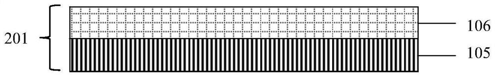
[0031] refer to figure 1 , figure 2 , using the radio frequency magnetron sputtering method to deposit a layer of double-layer TCO film 201 with a specific superposition structure on the front of the SHJ solar cell, the specific operation method includes the following steps:
[0032] (1) cleaning and texturizing the n-type monocrystalline silicon wafer to obtain a clean silicon wafer substrate with a pyramid structure on the surface;
[0033] (2) Depositing a layer of intrinsic amorphous silicon film passivation layer respectively on the front and back sides of the silicon wafer;
[0034] (3) Continue depositing one deck of n-type doped amorphous silicon film on the front side of the silicon wafer, and continue depositing one deck of p-type doped amorphous silicon film on the back side;
[0035] (4) Deposit a single-layer TCO film on the back side of the silicon wafer, i.e. on the p-type amorphous silicon film; on the front side of the silicon wafer, i.e. on the n-type amo...
Embodiment 2
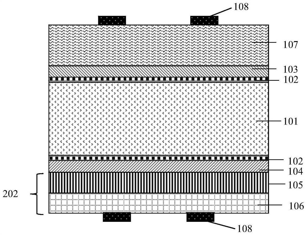
[0044] refer to figure 1 , image 3 , using the radio frequency magnetron sputtering method to deposit a layer of double-layer TCO film 202 with a specific superposition structure on the back of the SHJ solar cell, the specific operation method includes the following steps:
[0045] (1) cleaning and texturizing the n-type monocrystalline silicon wafer to obtain a clean silicon wafer substrate with a pyramid structure on the surface;
[0046] (2) Depositing a layer of intrinsic amorphous silicon film passivation layer respectively on the front and back sides of the silicon wafer;
[0047] (3) Continue depositing one deck of n-type doped amorphous silicon film on the front side of the silicon wafer, and continue depositing one deck of p-type doped amorphous silicon film on the back side;
[0048] (4) Deposit a single-layer TCO film on the front side of the silicon wafer, i.e. on the n-type amorphous silicon film; on the back side of the silicon wafer, i.e. on the p-type amorp...
Embodiment 3
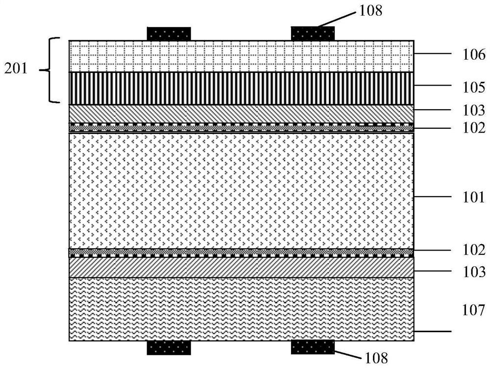
[0057] refer to figure 1 , Figure 4 , using the radio frequency magnetron sputtering method to deposit a layer of double-layer TCO thin film 201 / 202 with a specific superimposed structure on both sides of the SHJ solar cell. The specific operation method includes the following steps:
[0058] (1) cleaning and texturizing the n-type monocrystalline silicon wafer to obtain a clean silicon wafer substrate with a pyramid structure on the surface;
[0059] (2) Depositing a layer of intrinsic amorphous silicon film passivation layer respectively on the front and back sides of the silicon wafer;
[0060] (3) Continue depositing one deck of n-type doped amorphous silicon film on the front side of the silicon wafer, and continue depositing one deck of p-type doped amorphous silicon film on the back side;
[0061] (4) Deposit a columnar TCO film with a thickness of 20 nm on both sides of the silicon wafer, and then deposit a layer of equiaxed TCO film with a thickness of 80 nm to fo...
PUM
| Property | Measurement | Unit |
|---|---|---|
| Layer thickness | aaaaa | aaaaa |
| Total thickness | aaaaa | aaaaa |
| Power supply | aaaaa | aaaaa |
Abstract
Description
Claims
Application Information