Two-dimensional area array ultrasonic transducer and manufacturing method thereof

An ultrasonic transducer and array technology, used in ultrasonic therapy, ultrasonic/sonic/infrasonic diagnosis, sonic diagnosis, etc., can solve the problem of difficulty in cutting through, the impact of ultrasonic transducer performance and life, the difficulty of lead welding process, etc. problems, to achieve the effect of simplifying complexity, good heat dissipation, and improving reliability

Inactive Publication Date: 2016-03-23
SHENZHEN INST OF ADVANCED TECH CHINESE ACAD OF SCI
View PDF5 Cites 47 Cited by
  • Summary
  • Abstract
  • Description
  • Claims
  • Application Information

AI Technical Summary

Problems solved by technology

[0005] 2. In the existing wiring scheme, the matching layer and the backing material must use conductive materials, which not only makes the selection space of the matching layer and the backing material very narrow, but also limits the use of ultrasonic transducers in certain environments (such as magnetic resonance environment) applications
[0006] 3. In the existing wiring scheme, the leads are connected to the matching layer and the backing, so it is necessary to separate the matching layer and the backing, because the total thickness of the matching layer, the piezoelectric layer, and the backing is relatively It is difficult to cut through the process conditions. This solution

Method used


Image

  • Two-dimensional area array ultrasonic transducer and manufacturing method thereof
  • Two-dimensional area array ultrasonic transducer and manufacturing method thereof
  • Two-dimensional area array ultrasonic transducer and manufacturing method thereof

Examples


Embodiment Construction

[0029] The technical means adopted by the present invention to achieve the intended invention purpose are further described below in conjunction with the drawings and preferred embodiments of the present invention.

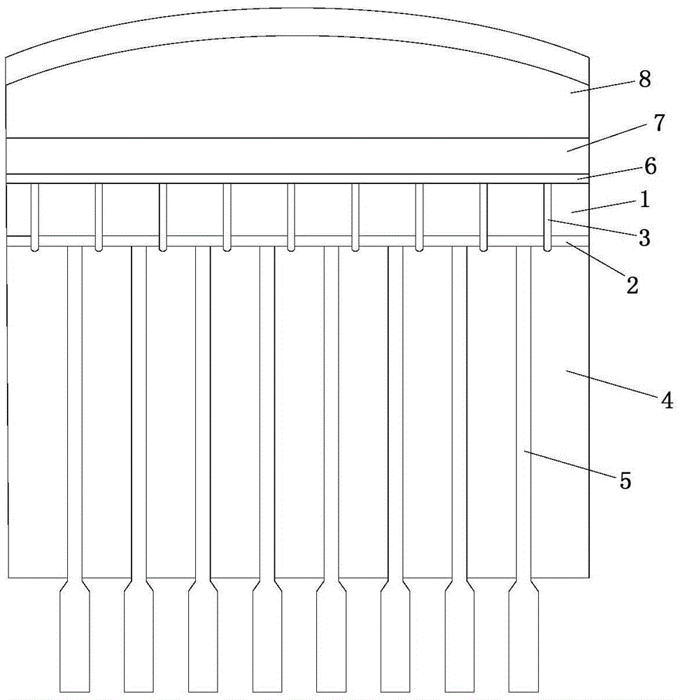
[0030] figure 1 It is a schematic structural diagram of a two-dimensional surface array ultrasonic transducer according to an embodiment of the present invention. Such as figure 1 As shown, the two-dimensional area array ultrasonic transducer includes:

[0031]The piezoelectric array element array layer 1 is formed by M×N piezoelectric array elements, and each piezoelectric array element is separated by a slit for receiving or transmitting ultrasonic signals. Wherein, the piezoelectric array element array layer 1 is a piezoelectric monomer or a piezoelectric composite material; the piezoelectric composite material can be a 1-3 type piezoelectric composite material or a 2-2 type piezoelectric composite material, such as a PZT piezoelectric ceramics.

[0032] Th...


PUM


Abstract

The invention provides a two-dimensional area array ultrasonic transducer and a manufacturing method thereof. The two-dimensional area array ultrasonic transducer comprises a piezoelectric array element array layer, array element electrodes, decoupling materials, backing blocks, electrode leads, a public electrode and a matching layer, wherein the piezoelectric array element array layer is formed by arranging M*N piezoelectric array elements which are divided by joints and used for receiving or transmitting ultrasonic signals, the array element electrodes are sputtered on the first surface of the piezoelectric array element array layer and cut and divided according to the joints, each array element electrode corresponds to one piezoelectric array element, the joints are filled with the decoupling materials which are used for lowering crosstalk interference of the piezoelectric array elements, the backing blocks are stuck to the array element electrodes and used for absorbing sound energy of the back faces of the piezoelectric array elements, the electrode leads are arranged on the backing blocks, the public electrode is sputtered on the second surface of the piezoelectric array element array layer, and the matching layer is stuck to the public electrode and used for achieving impedance matching between the piezoelectric array elements and external objects.

Description

technical field [0001] The invention relates to the field of preparation of ultrasonic imaging equipment, in particular to a two-dimensional surface array ultrasonic transducer and a preparation method thereof. Background technique [0002] Ultrasound transducers are key components in ultrasound equipment and can be used for ultrasound imaging, ultrasound stimulation, ultrasound therapy, and more. After the structure of the ultrasonic transducer has experienced the process of developing from a single vibration element to a linear array, a convex array, and a circular array, it is developing in the direction of a two-dimensional array. Since the birth of ultrasonic transducers, the earliest ones are single-array element ultrasonic transducers. Ultrasound images can be acquired by mechanically scanning (eg, sector scanning) a single-element ultrasound transducer. With the increasing maturity of the processing technology, the acquisition of two-dimensional ultrasonic images i...

Claims


Application Information

Patent Timeline
IPC IPC(8): A61B8/00A61N7/02
CPCA61B8/4488A61B8/0808A61N7/02
Inventor 钱明郑海荣李永川苏敏邱维宝
Owner SHENZHEN INST OF ADVANCED TECH CHINESE ACAD OF SCI
Why Eureka
Try Eureka