Light-emitting diode and method of making the same

A technology for light-emitting diodes and manufacturing methods, applied in electrical components, circuits, semiconductor devices, etc., can solve the problems of product quality influence, luminous intensity difference, uneven current expansion, etc., and achieve LED reliability improvement, uniform light emission, and enhanced current. The effect of expansion

Active Publication Date: 2018-04-10
TIANJIN SANAN OPTOELECTRONICS
View PDF3 Cites 0 Cited by
  • Summary
  • Abstract
  • Description
  • Claims
  • Application Information

AI Technical Summary

Problems solved by technology

However, due to structural design reasons, the current spread is uneven, that is, the luminous intensity of different positions of the same core particle will be different, and the overall luminous intensity will gradually increase from the P electrode to the N electrode. This phenomenon is manifested on large-sized core particles. will be particularly prominent, such as figure 1 As shown; on small-sized products, such as finished display screens, it will also have a certain impact on the quality of the finished product

Method used


Image

  • Light-emitting diode and method of making the same
  • Light-emitting diode and method of making the same
  • Light-emitting diode and method of making the same

Examples


Embodiment

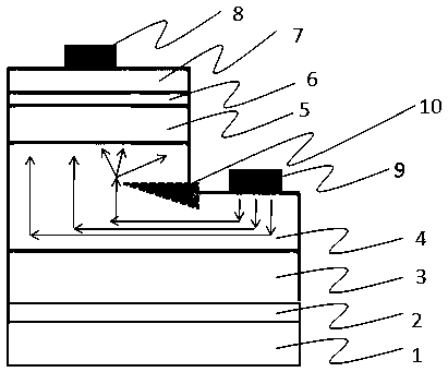
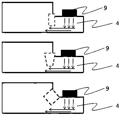
[0020] figure 2 It is a schematic diagram of a diode structure with uniform luminous intensity implemented according to the present invention. The epitaxial layer preparation process in this embodiment includes from bottom to top: (1) sapphire substrate 1; (2) low-temperature buffer layer 2, which can be nitrided Gallium, aluminum nitride, or aluminum-gallium-nitride combination, with a film thickness between 10 and 100 μm; (3) non-doped gallium nitride layer 3, with a film thickness between 300 and 7000 μm, preferably 3500 μm; (4) N-type layer 4. The thickness is greater than 1 μm; (5) The multi-quantum well active region 5 is composed of InGaN as the well layer and GaN or AlGaN or a combination of the two as the barrier layer, wherein the thickness of the barrier layer is between 50 and 150 nm, and the thickness of the well layer is Between 1~20nm; (6) Al x Ga 1-x The N electron blocking layer (where 0≤x≤1) has a thickness of ≤1 μm; (7) the P-type layer 7 has a thickness ...


PUM


Abstract

The invention provides a diode structure design with uniform luminous intensity. An epitaxial wafer structure comprises a substrate, an N-type layer, a multi-quantum well active region and a P-type layer from bottom to top; preparation of a chip technology is carried out; a current adjusting structure is arranged at the position, close to an N electrode, in the N-type layer; a resistance value of a region at the position, close to the N electrode, in the N-type layer is increased by the current adjusting structure; the current carrier aggregation effect of the position close to the N electrode is reduced by controlling the summarized occupied volume and the transverse and longitudinal etching depths of the current adjusting structure in the N-type layer; relatively multiple current carriers flow to the position close to a P electrode; the number of electrons which flow to the position close to the P electrode in the N-type layer is increased; different positions of a same LED chip are relatively uniform in light-emitting; and meanwhile, the current carrier aggregation effect is relieved, so that the reliability of an LED is further improved.

Description

technical field [0001] The invention relates to the field of gallium nitride semiconductor devices, in particular to the design and preparation of a diode structure with uniform luminous intensity. Background technique [0002] Light Emitting Diode (English for Light Emitting Diode, abbreviated as LED) is a semiconductor solid-state light-emitting device, which uses a semiconductor PN junction as a light-emitting structure. Gallium nitride is currently regarded as the third-generation semiconductor material, with InGaN / GaN active regions Gallium nitride-based light-emitting diodes are regarded as the most potential light-emitting source today. [0003] In commercialized LED factories, epitaxial wafers grown on sapphire substrates are mostly made into horizontal structure chips. However, due to structural design reasons, the current spread is uneven, that is, the luminous intensity at different positions of the same core particle will be different, and the overall luminous i...

Claims


Application Information

Patent Timeline
Patent Type & Authority Patents(China)
IPC IPC(8): H01L33/14H01L33/20H01L33/00
CPCH01L33/0066H01L33/0075H01L33/14H01L33/20
Inventor 舒立明王良均刘晓峰叶大千吴超瑜王笃祥
Owner TIANJIN SANAN OPTOELECTRONICS
Why Eureka
Try Eureka