
Digital circuit design method and related system

A digital circuit and design method technology, applied in the direction of electrical digital data processing, calculation, special data processing applications, etc., can solve the problems of circuit program files that cannot be matched with simulation, errors, difficulties, etc.

Active Publication Date: 2016-03-30
REALTEK SEMICON CORP
View PDF4 Cites 5 Cited by
  • Summary
  • Abstract
  • Description
  • Claims
  • Application Information

AI Technical Summary

Problems solved by technology

[0003] Generally speaking, it is not necessary to do functional simulation with timing delay information after logic synthesis until the physical design is completed, and it is also difficult to do such simulation. For example, in the setting of logic synthesis, in the circuit Nodes with a high number of loads (highfan-outnet) will be marked with a huge delay time in the timing information (timinginformation) generated by logic synthesis, so that the circuit program file (netlist) generated by logic synthesis cannot be matched The timing information is used to simulate
[0004] The above-mentioned nodes with high load numbers will undergo additional processing in the subsequent physical design so that the delay time will not be too long. However, if the post-circuit layout simulation is to be performed after the physical design is completed, because this time point It is usually close to the time of tapeout. Therefore, if the problem is discovered after the circuit layout is simulated, it will often affect the product schedule.
[0005] For digital design, if the constraints set during logic synthesis are correct and sufficient, and the correct static timing analysis (static timing analysis) is verified accordingly, generally speaking, the simulation after circuit layout is not too difficult. Mistakes will occur. However, sometimes due to the mistakes that engineers make when inputting constraints, the mistakes are not found during the static timing analysis, but are discovered after the circuit layout is simulated, or some design mistakes May also escape static timing analysis only to be discovered after simulation after circuit layout
However, as mentioned in the previous paragraph, waiting until after the physical design is complete to discover such errors is usually too late

Method used


Image

  • Digital circuit design method and related system
  • Digital circuit design method and related system

Examples


Embodiment Construction

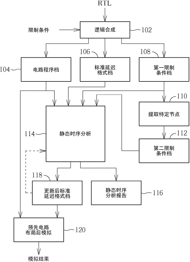
[0015] Please refer to figure 1 , figure 1 It is a flowchart of a digital circuit design method according to an embodiment of the present invention. In this embodiment, the digital circuit design method is executed by a plurality of program instruction modules after a system for digital circuit design is loaded into a computer / processor, refer to figure 1 , the flow of the digital circuit design method is described as follows.

[0016] First, in step 102, a logic synthesis (logics synthesis) operation is performed according to a Register Transfer Level (RTL) design and a plurality of constraints (constraints), so as to generate a circuit program file ( netlist), a standard delay format file (StandardDelayFormat, SDF), and a first constraint file (constraintfile). The above constraints are input by the engineer, and mainly include which pin is the clock input point, and what is the frequency of the clock...etc.; the circuit program file is a file format describing the circui...


PUM


Abstract

The invention provides a digital circuit design method and a related system. The digital circuit design method comprises the following steps: before performing substantive design, performing logic synthesis according to the transfer-level design of a register and multiple constraints so as to at least generate a netlist file, a standard delay format file, and a first constraint file; extracting information of at least one specific node in a circuit from the first constraint file so as to generate a second constraint file; generating an updated standard delay format file at least according to the standard delay format file and the second constraint file, wherein the delay amount of the specific node in the updated standard delay format file is less than that of the specific node in the standard delay format file; and performing advance circuit post-layout simulation by using the netlist file and the updated standard delay format file.

Description

technical field [0001] The invention relates to the technical field of circuit design, in particular to a digital circuit design method and a related system. Background technique [0002] The traditional digital circuit design is mainly divided into the front section and the back section. The front section mainly includes the register transfer level (Register Transfer Level, RTL) design, functional simulation (functional simulation), and logic synthesis (logics synthesis), while the back section includes the Physical design, automatic circuit layout, and postlayout simulation (postlayoutsimulation), etc. [0003] Generally speaking, it is not necessary to do functional simulation with timing delay information after logic synthesis until the physical design is completed, and it is also difficult to do such simulation. For example, in the setting of logic synthesis, in the circuit Nodes with a high number of loads (highfan-outnet) will be marked with a huge delay time in the ...

Claims


Application Information

Patent Timeline
Patent Type & Authority Applications(China)
IPC IPC(8): G06F17/50
Inventor 曾顺得翁启舜
Owner REALTEK SEMICON CORP
Learn More