
Modelling method for surface potential basis intensive model of III-V group HEMT (High Electron Mobility Transistor)

A modeling method and surface potential technology, applied in special data processing applications, instruments, electrical digital data processing, etc., can solve problems such as discontinuous segment points, charge equations that cannot be integrated, and nonlinear circuit simulations that cannot be used

Active Publication Date: 2016-04-06
HANGZHOU DIANZI UNIV
View PDF3 Cites 21 Cited by
  • Summary
  • Abstract
  • Description
  • Claims
  • Application Information

AI Technical Summary

Problems solved by technology

[0003] The purpose of the present invention is to address the shortcomings of the existing III-V group HEMT device modeling technology, to provide a modeling method for the III-V group HEMT surface potential base intensive model, aiming to solve the existing III-V group The current and charge equations of HEMT devices cannot be integrated, the segment points are discontinuous, and they cannot be used for nonlinear circuit simulation, etc. Establish an accurate III-V HEMT intensive model

Method used


Image

  • Modelling method for surface potential basis intensive model of III-V group HEMT (High Electron Mobility Transistor)
  • Modelling method for surface potential basis intensive model of III-V group HEMT (High Electron Mobility Transistor)
  • Modelling method for surface potential basis intensive model of III-V group HEMT (High Electron Mobility Transistor)

Examples


Embodiment Construction

[0063] The present invention will be further tested, verified and analyzed below in conjunction with the accompanying drawings and specific examples.

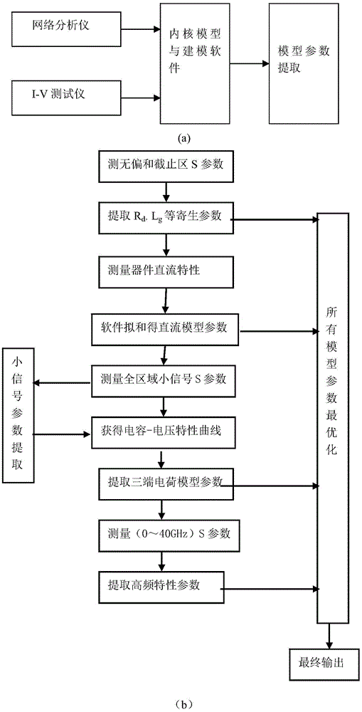
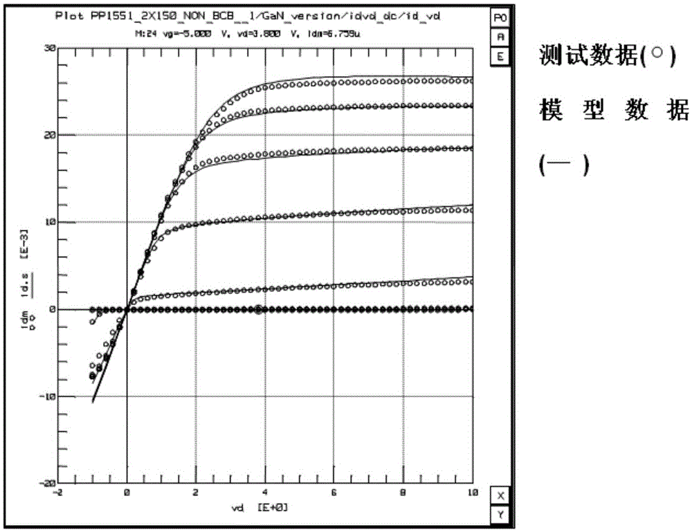
[0064] The AlGaN / GaN HEMT device is an important representative of the III-V HEMT device. The present invention carries out an intensive model establishment and model parameter extraction for a depletion-mode AlGaN / GaN HEMT device with 2 gate fingers, a gate length of 0.25um, and a gate width of 10um. CLP Group provides die test data. Such as figure 1 As shown, the modeling method of the AlGaN / GaNHEMT surface potential basis intensive model includes the following steps;

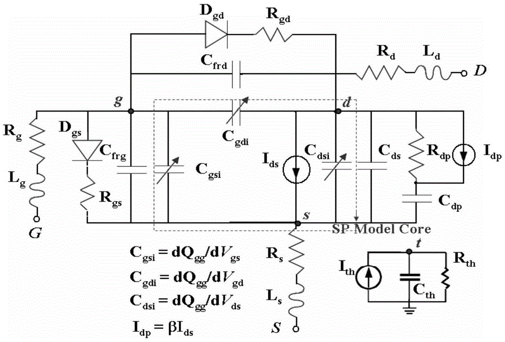
[0065] Step 1. Establish an AlGaN / GaNHEMT surface potential basis intensive kernel model:

[0066] 1.1 Write the unique polarization and quantum effects of AlGaN / GaNHEMT devices into the two-dimensional Poisson equation, derive the surface potential equation of the AlGaN / GaNHEMT device, realize the characterization of different structures of the device, and ...


PUM


Abstract

The invention discloses a modelling method for a surface potential basis intensive model of an III-V group HEMT (High Electron Mobility Transistor). The method comprises the following steps of firstly, establishing an intrinsic structure model and an extrinsic structure model of the III-V group HEMT, combining a physical structure and a behavior mechanism of a device to construct a topological structure, and then embedding the established models into a commercial EDA (Electronic Design Automation) tool; secondly, carrying out on-wafer testing on an actual depletion device to obtain various performance test data of the device; and lastly, verifying the intensive model. The model solves the problems that the existing current and charge equations of the device cannot integrate, the segment points are discontinuous and the equations cannot be used for nonlinear circuit simulation; through a method for solving a surface potential source equation to deduce model current and charge / capacitance equations, a physical problem for quantum effect processing and a numerical algorithm problem caused by simultaneous self-consistent solution of a classic carrier transport equation and a new effect in the existing physical model are solved; and furthermore, a computational formula for volume charge density is deducted again, so that a problem of difficulty in gluing in a charge model is solved.

Description

technical field [0001] The invention relates to a microelectronic device modeling technology, in particular to a modeling method of a III-V family HEMT surface potential basis intensive model. Background technique [0002] III-Ⅴ group high electron mobility transistor (HEMT) is recognized as the most competitive three-terminal device in the field of microwave / millimeter wave devices and circuits. At present, low-noise amplifiers and power amplifiers made of III-Ⅴ HMET have been Widely used in satellite receiving systems, electronic radar systems and optical fiber communication systems. However, as the basis of microwave monolithic integrated circuit computer-aided design (MMICAD), the III-V HEMT device models suitable for large-scale electronic design automation (EDA) simulation applications are still scarce, and the development of modeling technology lags behind. The feasibility and precision of the model and modeling technology are the key to the success of MMICAD. The l...

Claims


Application Information

Patent Timeline
IPC IPC(8): G06F17/50
CPCG06F30/39G06F30/398
Inventor 汪洁刘军孙玲玲
Owner HANGZHOU DIANZI UNIV
Learn More