Back-gate field effect transistor based on contact electrification

A field-effect transistor and contact electrification technology, which is applied in the direction of circuits, electrical components, semiconductor devices, etc., can solve the problems of selection and application restrictions, and achieve the effects of simple structure, easy fabrication and integration, and wide external force sensing range

Active Publication Date: 2016-04-06
BEIJING INST OF NANOENERGY & NANOSYST
View PDF5 Cites 14 Cited by
  • Summary
  • Abstract
  • Description
  • Claims
  • Application Information

AI Technical Summary

Problems solved by technology

However, piezoelectric electronic transistors must be prepared with piezoelectric materials, and the controllability of the piezoelectric potential generated by them, as well as the selection and application of materials, are subject to many restrictions.

Method used


Image

  • Back-gate field effect transistor based on contact electrification
  • Back-gate field effect transistor based on contact electrification
  • Back-gate field effect transistor based on contact electrification

Examples


no. 1 example

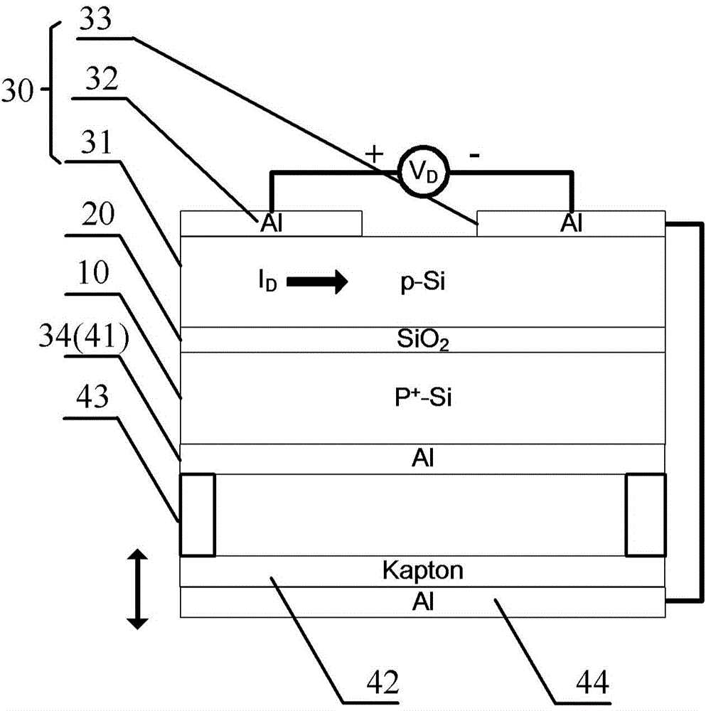
[0035] In a first exemplary embodiment of the present invention, a back gate field effect transistor based on contact electrification is provided. figure 1 It is a schematic structural diagram of a back gate field effect transistor based on contact electrification according to the first embodiment of the present invention. Such as figure 1 As shown, the back gate field effect transistor based on contact electrification in this embodiment includes: a conductive substrate 10; an insulating layer 20 formed on the front surface of the conductive substrate 10; a field effect transistor assembly 30 including: a channel layer 31 formed on the insulating layer The top of the layer 20; the drain 32 and the source 33 are formed above the channel layer 31, the two are separated by a preset distance, and a preset potential difference is maintained; the gate 34 is formed on the back of the conductive substrate 10; The triboelectric power generation assembly 40 includes: a static friction ...

no. 3 example

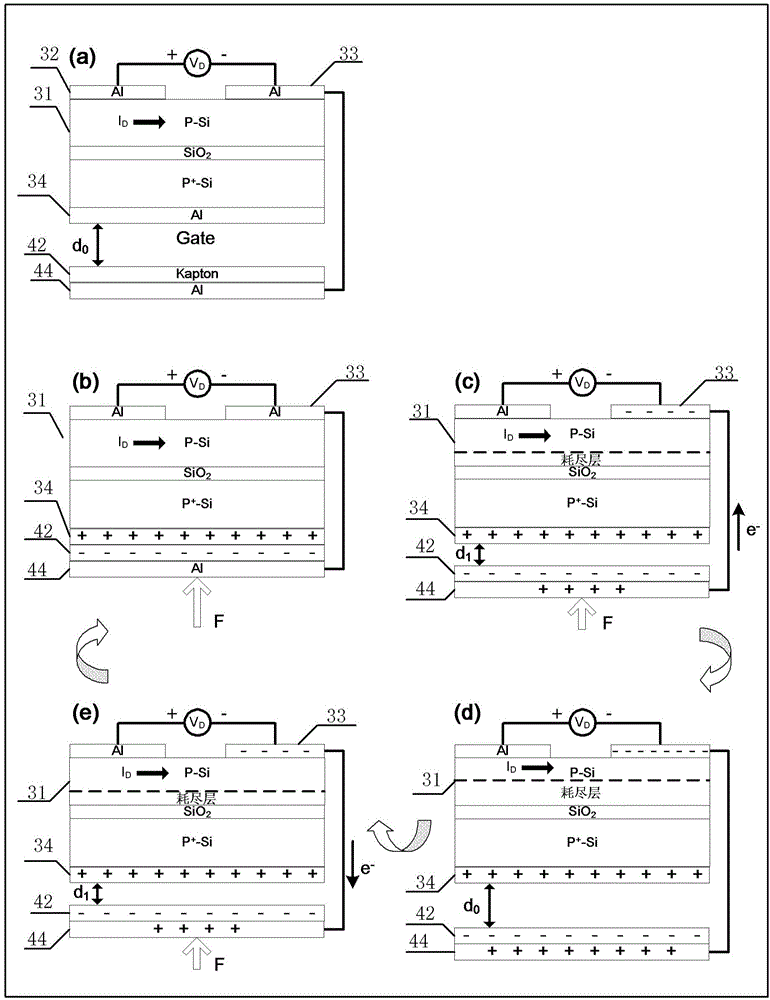
[0075] In the third exemplary embodiment of the present invention, another back gate field effect transistor based on contact electrification is also provided. Figure 5 It is a schematic structural diagram of a back gate field effect transistor based on contact electrification according to the third embodiment of the present invention. Such as Figure 5 As shown, the back gate field effect transistor based on contact electrification in this embodiment is similar to the structure of the first embodiment, the difference is that the static friction layer is made of polyimide polymer material, fixed on the gate 34, and can move The friction layer is an aluminum plate, which is isolated from the static friction layer by springs, and the aluminum plate is directly electrically connected to the source 33 through wires.

[0076] Figure 6 for Figure 5 Schematic diagram of the operation of the back-gate field-effect transistor shown. Combine the following Figure 6 To introduce ...


PUM


Abstract

The invention provides a back-gate field effect transistor based on contact electrification. The back-gate field effect transistor comprises the components of a conductive substrate; an insulating layer which is formed on the front surface of the conductive substrate; a field effect transistor assembly which comprises a channel layer, a drain electrode, a source electrode and a gate electrode; and a friction electrification assembly. The friction electrification assembly comprises the components of a static friction layer which is formed on the lower surface of the gate electrode; a movable friction layer which is separated from the static friction layer and is arranged parallelly with the static friction layer; and a second conductive layer which is formed outside the movable friction layer and is electrically connected with the source electrode, wherein the static friction layer and the movable friction layer are arranged at different positions of a friction electrode set. In response to the function of an external force, the static friction layer and the movable friction layer can be repeatedly switched between a separating state and a contacting state. According to the back-gate field effect transistor, an electrostatic potential which is generated by a friction electrification machine is used as a gate electrode gate signal of the back-gate field effect transistor, thereby realizing control for transportation characteristic of carriers in a semiconductor.

Description

technical field [0001] The invention relates to the technical field of electronic components in the electronics industry, in particular to a back gate field effect transistor based on contact electrification. Background technique [0002] Field effect transistors are based on transistor devices that control the current transport process in the element by using a gate voltage. The metal-oxide-semiconductor field-effect transistor (MOSFET) based on the back gate SOI structure has simple structure, low electric field, high transconductance and good short channel characteristics, and its back substrate can be used as the back gate, and the back gate voltage to tune the width of the conductive channel in the top silicon. Although the field effect transistor technology is very mature, in view of the three-terminal structure of the device unit, the grid power supply needs to be specially provided, and the integration is complicated, and the pressure sensing device based on this ty...

Claims


Application Information

Patent Timeline
Patent Type & Authority Applications(China)
IPC IPC(8): H01L29/808H01L29/423
CPCH01L29/42384H01L29/4908H01L29/4916H01L29/78603H01L29/78654H01L29/84H01L29/42356H10N30/1051H10N30/30H10N30/50H01L29/423H01L29/78H01L23/535H01L29/0649H01L29/36
Inventor 张弛唐伟张丽敏王中林
Owner BEIJING INST OF NANOENERGY & NANOSYST
Why Eureka
Try Eureka