Preparation method of polyolefin nanometer electric composite dielectric material SEM analysis sample

A composite medium and analysis sample technology, which is used in the preparation of test samples, material analysis using wave/particle radiation, and analysis of materials, etc., can solve the problem that the sample is not flat enough, the surface information is real, and the polyolefin cannot be distinguished. Nanoparticles and other problems to achieve the effect of eliminating the impact

Inactive Publication Date: 2016-04-13
HARBIN UNIV OF SCI & TECH
View PDF7 Cites 3 Cited by
  • Summary
  • Abstract
  • Description
  • Claims
  • Application Information

AI Technical Summary

Problems solved by technology

[0005] The invention solves the problem that when using SEM to observe the microstructure of the polyolefin nanoelectric composite dielectric material, because the sample is not smooth enough, the information of the unevenness affects us to obtain the image, and the real situation of the surface information cannot be well characterized, and even The technical problem of being unable to distinguish the nanoparticles on the surface of the polyolefin nanoelectric composite dielectric material; and providing a preparation method for the SEM analysis sample of the polyolefin nanoelectric composite dielectric material

Method used


Image

  • Preparation method of polyolefin nanometer electric composite dielectric material SEM analysis sample
  • Preparation method of polyolefin nanometer electric composite dielectric material SEM analysis sample
  • Preparation method of polyolefin nanometer electric composite dielectric material SEM analysis sample

Examples


specific Embodiment approach 1

[0023] Specific Embodiment 1: In this embodiment, polyolefin nanoelectric composite dielectric materials are prepared from polypropylene particles and nano-silica with a particle size of 50 nm; the specific method is as follows: polypropylene particles and nano-silica with a particle size of 50 nm Place them in evaporating dishes respectively (the evaporating dish containing polyolefin particles is not covered, and the evaporating dish containing nanomaterials is covered), the temperature of the drying oven is set at 50°C, and the drying time is 24h; Polyethylene particles and nano-silica were mixed at a mass ratio of 100:1, the heating temperature of the torque rheometer was set at 190°C, and the mixing time was 20 minutes; a polyolefin nanoelectric composite dielectric material was obtained.

[0024] In the present embodiment, the preparation method of polyolefin nanoelectric composite dielectric material SEM analysis sample is completed by the following steps:

[0025] Step...

specific Embodiment approach 2

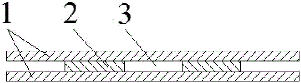
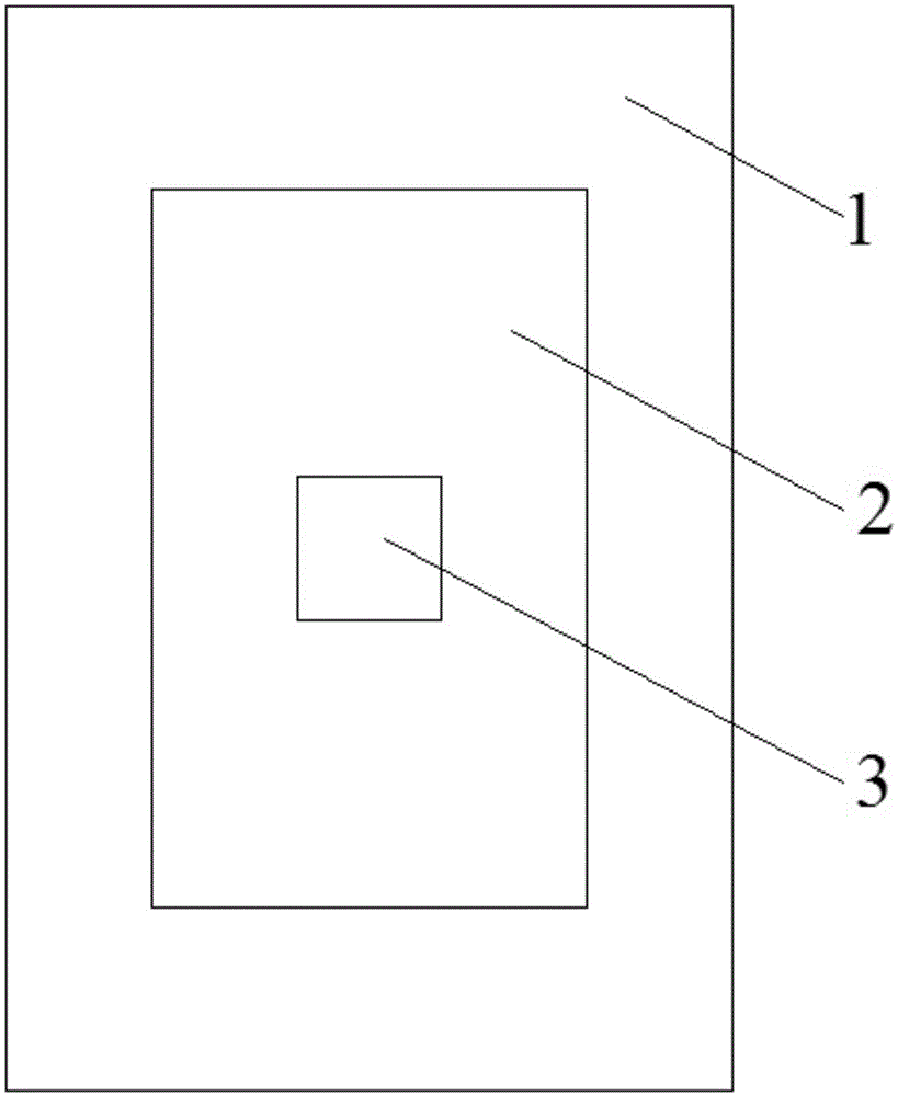
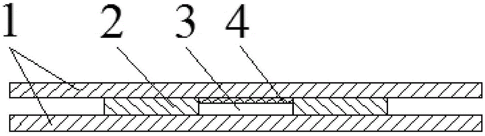
[0031] Specific embodiment two: the difference between this embodiment and specific embodiment one is: in step 2, a metal mesh with a mesh number of 100 is placed on the sheet sample (see image 3 ). Other steps and parameters are the same as in the first embodiment.


PUM

PropertyMeasurementUnit
thicknessaaaaaaaaaa
particle sizeaaaaaaaaaa

Abstract

The invention discloses a preparation method of a polyolefin nanometer electric composite dielectric material SEM analysis sample, and belongs to the field of surface topography analysis. The technical problems that when an SEM is used for observing a microstructure of a polyolefin nanometer electric composite dielectric material, due to the fact that a sample is not level or smooth enough, the non-level and unsmooth information affects people obtaining images, the true circumstance of surface information cannot be well represented, and even nanometer particles on the surface of the polyolefin nanometer electric composite dielectric material cannot be recognized are solved. The method comprises the steps that 1, the polyolefin nanometer electric composite dielectric material is dried; 2, the dried polyolefin nanometer electric composite dielectric material is placed on a press vulcanizer to be pressed into a sheet and sheared to obtain a sheet sample; 3, an assembly to be pressed is assembled; 4, the assembly to be pressed is placed in the press vulcanizer to be pressed for the second time, a heating power source of the press vulcanizer is turned off, the product is naturally cooled along with the press vulcanizer, and the product is taken out of the press vulcanizer to be stored. The sample is used for SEM analysis of the polyolefin nanometer electric composite dielectric material.

Description

technical field [0001] The invention belongs to the field of surface morphology analysis, in particular to a method for preparing a sample for SEM analysis of a polyolefin nanoelectric composite dielectric material. Background technique [0002] Since filling nanomaterials can improve some basic properties of dielectric materials, polyolefin nanoelectric composite dielectric materials have gradually become a research hotspot in the field of dielectrics. Because ordinary optical microscopes cannot observe fillers with a scale of nanometers, scanning electron microscopy It has become an essential means to characterize the morphology of dielectric nanocomposites. [0003] The basic principle of the scanning electron microscope is: under the action of accelerating high voltage, the electrons emitted by the electron gun are collected into a small (generally 1-5nm in diameter) electron beam (the corresponding beam current is 10 nm) through a multi-stage electromagnetic lens. -11 ...

Claims


Application Information

Patent Timeline
Patent Type & Authority Applications(China)
IPC IPC(8): G01N1/28
CPCG01N23/2202
Inventor 王暄崔林杨佳明
Owner HARBIN UNIV OF SCI & TECH
Why Eureka
Try Eureka