
TFT (thin film transistor) array substrate

A technology of array substrates and substrate substrates, which is applied in the directions of optics, instruments, electrical components, etc., can solve the problems of difficult changes and the inability to increase the capacity of storage capacitors, and achieve the goals of improving crosstalk, improving display quality, and increasing capacity Effect

Inactive Publication Date: 2016-04-13
WUHAN CHINA STAR OPTOELECTRONICS TECH CO LTD
View PDF11 Cites 22 Cited by
  • Summary
  • Abstract
  • Description
  • Claims
  • Application Information

AI Technical Summary

Problems solved by technology

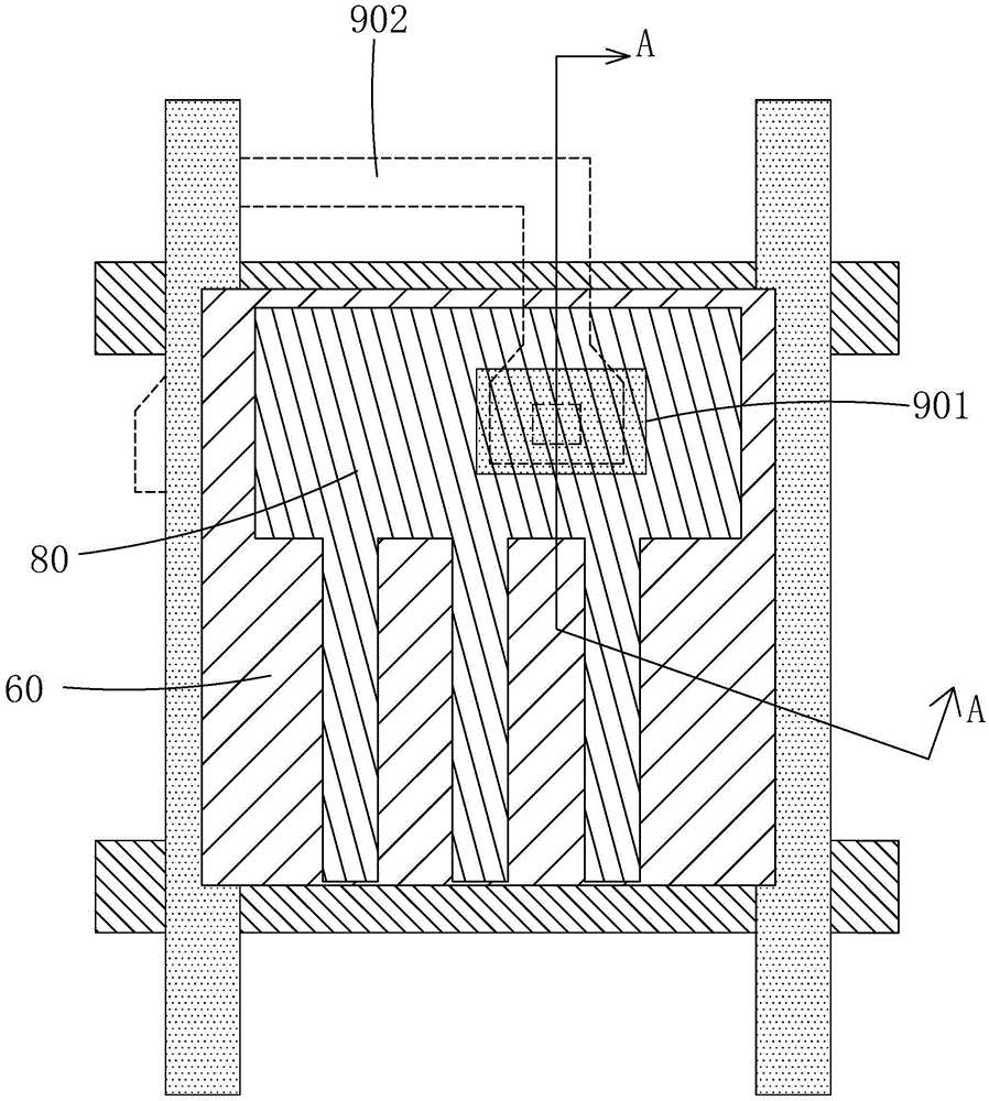
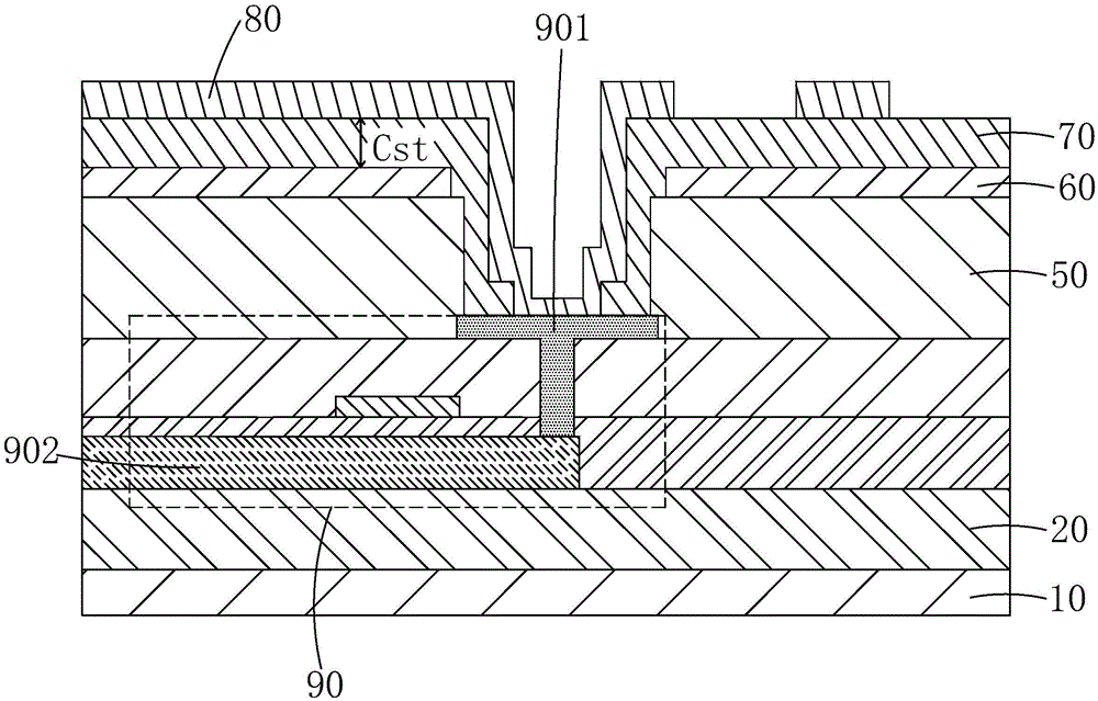
like figure 1 and figure 2 The existing TFT array substrate shown is limited by the requirements of process capability, optical quality and transmittance, and it is difficult to change the area of ​​the patterned pixel electrode 80, and it is impossible to increase the area of ​​the pixel electrode 80 to achieve this effect. ways to increase the capacity of the storage capacitor

Method used


Image

  • TFT (thin film transistor) array substrate
  • TFT (thin film transistor) array substrate
  • TFT (thin film transistor) array substrate

Examples


no. 1 example

[0039] see Figure 4 and Figure 6 , in order to further increase the storage capacitance, in the second embodiment of the TFT array substrate of the present invention, the thickness of the flat layer 500 located in the area where the drain electrode 420 overlaps with the horizontal projection of part of the common electrode 600 is smaller than that located in the The thickness of the planar layer 500 outside the region where the horizontal projection of the drain electrode 420 overlaps with part of the common electrode 600 can specifically be fabricated with different thicknesses of the planar layer 500 by exposing with a half-tone mask. Compared with the first embodiment, the second embodiment reduces the distance between one electrode plate (common electrode 600) and the other electrode plate (drain 420) of the first capacitor Cst1, thereby further increasing the distance between the first capacitor Cst1 A capacity of the capacitor Cst1. Preferably, the thickness of the p...


PUM


Abstract

The invention provides a TFT (thin film transistor) array substrate. Through increase of the area of a drain (420) of each TFT (900) located in a shading area, the horizontal projection of the drain (420) is overlapped with the horizontal projection of part of a corresponding common electrode (600), and the drain (420) and the common electrode (600) constitute a first memory capacitor (Cst1), a corresponding pixel electrode (800) and the common electrode (600) constitute a second memory capacitor (Cst2), the pixel electrode (800) and the drain (420) are contacted to form electrical connection and are isopotential, the first memory capacitor (Cst1) and the second memory capacitor (Cst2) are connected in parallel to constitute a memory capacitor, and the capacity of the memory capacitor is equal to the capacity sum of the first memory capacitor (Cst1) and the second memory capacitor (Cst2). Under the premise that the aperture rate is not reduced, the capacity of the memory capacitor can be increased, the problems of crosstalk interference, image sticking and the like are solved, and the display quality of a product is improved.

Description

technical field [0001] The present invention relates to the field of display technology, in particular to a TFT array substrate. Background technique [0002] Liquid Crystal Display (LCD) has many advantages such as thin body, power saving, and no radiation, and has been widely used, such as: LCD TV, mobile phone, personal digital assistant (PDA), digital camera, computer screen or notebook computer Screens, etc., dominate the field of flat panel displays. [0003] Most of the liquid crystal displays currently on the market are backlight liquid crystal displays, which include a liquid crystal display panel and a backlight module. The working principle of the liquid crystal display panel is to pour liquid crystal molecules between the thin film transistor array substrate (ThinFilmTransistorArraySubstrate, TFTArraySubstrate) and the color filter substrate (ColorFilter, CF), and apply a driving voltage on the two substrates to control the rotation of the liquid crystal molecul...

Claims


Application Information

Patent Timeline
Patent Type & Authority Applications(China)
IPC IPC(8): G02F1/1362
CPCG02F1/136213H01L27/1255H01L27/1222H01L27/124H01L27/1248H01L29/456H01L29/4908H01L29/495H01L29/78633H01L29/78675
Inventor 刘元甫
Owner WUHAN CHINA STAR OPTOELECTRONICS TECH CO LTD
Learn More