Large power semiconductor laser with stable light spots

A high-power, semiconductor technology, used in semiconductor lasers, optical waveguide semiconductor structures, lasers, etc., can solve problems that will affect the optical path, the impact of optoelectronic integration applications, and the addition of components.

Inactive Publication Date: 2016-04-13
Shandong Huaguang Optoelectronics Co. Ltd.
View PDF3 Cites 2 Cited by
  • Summary
  • Abstract
  • Description
  • Claims
  • Application Information

AI Technical Summary

Problems solved by technology

This method uses the external cavity mode selection method, which increases the number of components and affects the optical path, which will be affected in the application of optoelectronic integration

Method used


Image

  • Large power semiconductor laser with stable light spots
  • Large power semiconductor laser with stable light spots

Examples


Embodiment Construction

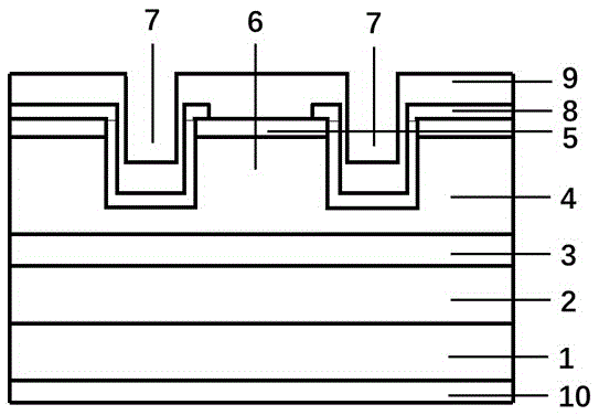
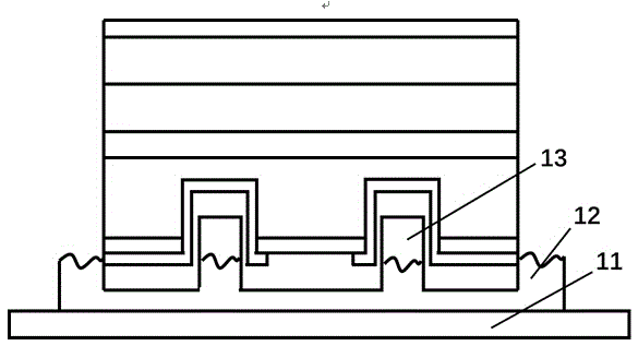
[0020] like figure 1 As shown, the spot-stabilized high-power semiconductor laser of the present invention includes a substrate 1 , a lower cladding layer 2 , an active region 3 , an upper cladding layer 4 and a contact layer 5 from bottom to top. Substrate 1 is a common GaAs substrate. The lower cladding layer 2, the active region 3 and the upper cladding layer 4 are made of AlGaInP material lattice-matched with the GaAs substrate, and the emission wavelength is about 650nm. The contact layer 5 is GaAs heavily doped with Zn, and the doping concentration is 1×10 19 ~1×10 20 cm -3 . The total thickness of the upper cladding layer 4 and the contact layer 5 is 2-3 μm.

[0021] A ridge structure 6 is formed on the upper cladding layer 4 and the contact layer 5 by wet etching or dry etching, and grooves 7 are formed on both sides of the ridge structure 6 . To satisfy high power output, the width of the ridge structure 6 is 50-150 μm, and the width of the groove 7 is 10-30 μm....


PUM

PropertyMeasurementUnit
Doping concentrationaaaaaaaaaa
Thicknessaaaaaaaaaa
Widthaaaaaaaaaa

Abstract

A large power semiconductor laser with stable light spots successively comprises a substrate, a lower wrapping layer, an active region, an upper wrapping layer and a contact layer from bottom to top. The upper wrapping layer and the contact layer are provided with a ridge-type structure. Channels are formed at two sides of the ridge-type structure. The depth of the channels is smaller than the total thickness of the upper wrapping layer and the contact layer. The part, except the ridge-type structure, on the upper surface of the contact layer and the surfaces of the channels are covered by dielectric films. The dielectric films and the ridge-type structure are covered by a first metal electrode layer. The bottom surface of the substrate is provided with a second metal electrode layer. The first metal electrode layer is sintered on a heat sink, and air isolation layers are arranged between a solder and the bottom parts of the channels. The upper wrapping layer of the laser is relatively thick, the ridge-type structure is prepared, lateral emission paths of heat generated by the active region in work are blocked by the air isolation layers, the heat is vertically emitted mainly through the ridge-type contact layer, so that the refractive index gradients of the middle part of the ridge-type structure and the active region close to the channel parts do not increase with the increasing of generated heat, and near-field light spots are more stable.

Description

technical field [0001] The invention relates to a high-power semiconductor laser with stable light spot, belonging to the technical field of semiconductor lasers. Background technique [0002] High-power semiconductor lasers have the advantages of small size, high integration, high electro-optic conversion efficiency, and low cost, and are widely used in material processing, laser printing and display, pumping solid-state and fiber lasers and other fields. These applications require that the optical power distribution of the laser is uniform and stable, that is, the near-field and far-field spots of the semiconductor laser are uniform, and the spot size does not change with current or temperature fluctuations. [0003] In order to ensure high power output and reliability, high-power semiconductor lasers generally use a wide-strip structure to reduce the optical power density and injection current density on the cavity surface. Different from semiconductor lasers with narrow...

Claims


Application Information

Patent Timeline
IPC IPC(8): H01S5/22H01S5/323
CPCH01S5/2207H01S5/2218H01S5/32316H01S5/32333
Inventor 朱振张新徐现刚
Owner Shandong Huaguang Optoelectronics Co. Ltd.
Why Eureka
Try Eureka