Wafer bonding method and wafer bonding structure
A wafer bonding and wafer technology, applied in the manufacture of electrical components, electrical solid devices, semiconductor/solid devices, etc., can solve the problems of 3D integrated circuit failure, short circuit, etc., and achieve the effect of reducing the risk of short circuit
- Summary
- Abstract
- Description
- Claims
- Application Information
AI Technical Summary
Problems solved by technology
Method used
Image

Examples
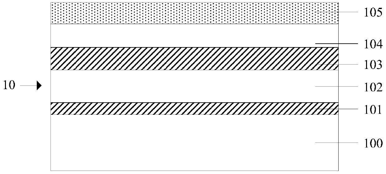
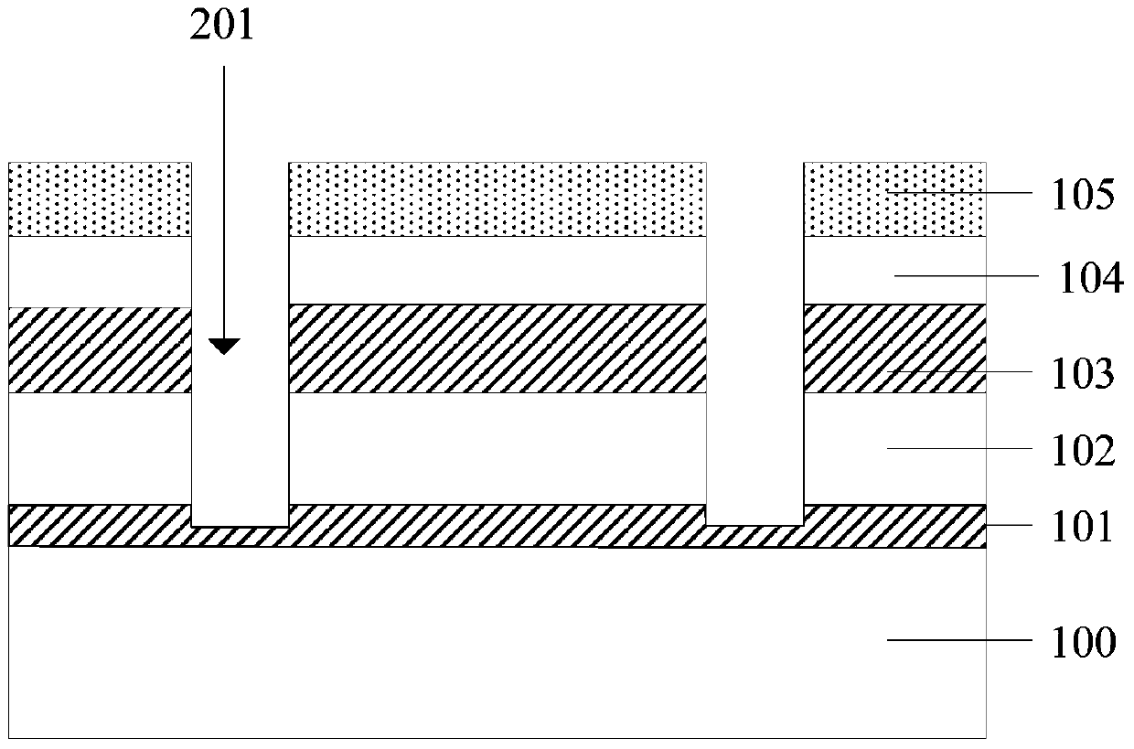
Embodiment Construction
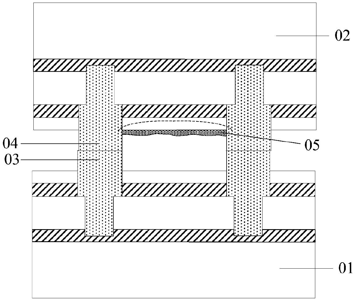
[0031] As mentioned in the background art, in the manufacturing process of 3D integrated circuits, after the wafer bonding process, a short circuit is likely to occur between bonded ends, which affects the bonding quality.
[0032] Analyze the cause of short circuit between the bonded ends, continue to refer to figure 1 As shown, since the distance between the first bonded ends 03 on the surface of the first wafer 01 is small, the distance between the second bonded ends 04 on the surface of the second wafer 02 is small, so that the first bonded ends 03 Or the metal ion in the second bonding end 04 such as figure 1 As shown by the dotted line in the middle, diffusion is easy to occur, so that a short circuit is likely to occur between adjacent first bonding ends 03 or between adjacent second bonding ends 04 .
[0033] In addition, the first bonding end 03 and the second bonding end 04 are usually made of copper material, and copper is easily corroded by oxygen and water vapor ...
PUM
| Property | Measurement | Unit |
|---|---|---|
| Thickness | aaaaa | aaaaa |
| Thickness | aaaaa | aaaaa |
Abstract
Description
Claims
Application Information
 - R&D
- Intellectual Property
- Life Sciences
- Materials
- Tech Scout
- Unparalleled Data Quality
- Higher Quality Content
- 60% Fewer Hallucinations
Browse by: Latest US Patents, China's latest patents, Technical Efficacy Thesaurus, Application Domain, Technology Topic, Popular Technical Reports.
© 2025 PatSnap. All rights reserved.Legal|Privacy policy|Modern Slavery Act Transparency Statement|Sitemap|About US| Contact US: help@patsnap.com