

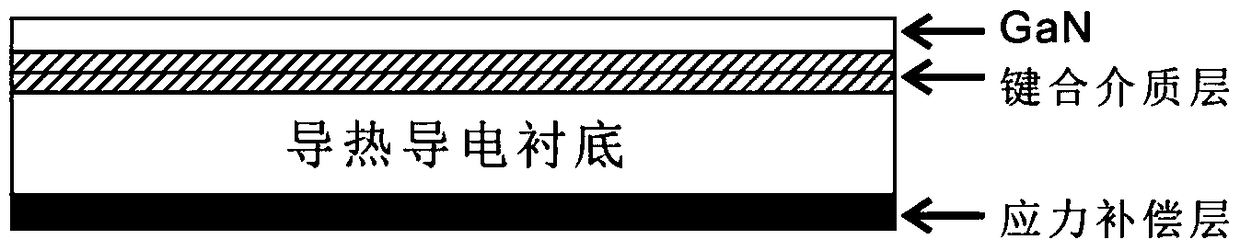
A low stress state composite substrate for gan growth
A composite substrate, low-stress technology, applied in semiconductor devices, electrical components, circuits, etc., can solve problems affecting the quality of homogeneous epitaxy and chip preparation, GaN epitaxial film wrinkles, poor high temperature stability, etc., to suppress substrate warping Curved and wrinkled epitaxial film, improved epitaxial growth quality, and good thermal and electrical conductivity
- Summary
- Abstract
- Description
- Claims
- Application Information
AI Technical Summary
Problems solved by technology
Method used
Image


Examples
Embodiment 1
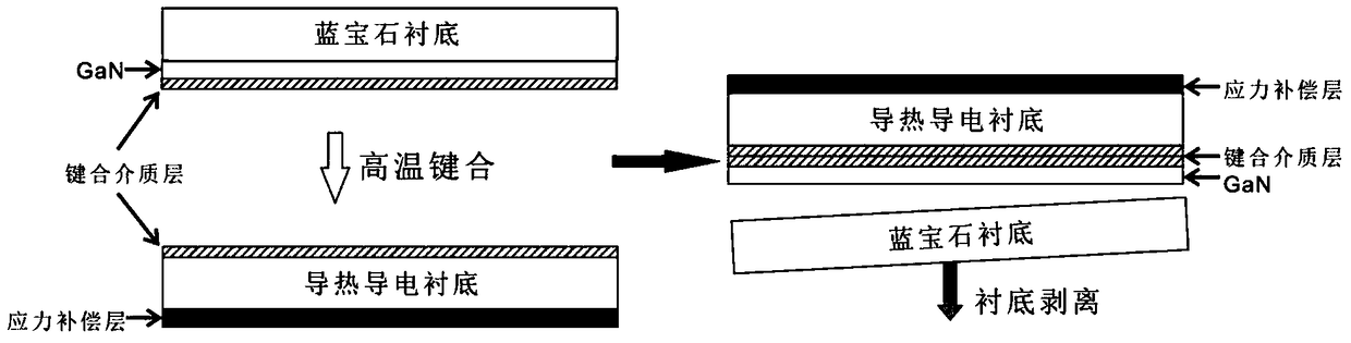
[0036] Embodiment 1: use Ni as the stress compensation layer, conductive Ag paste bonding CuMo metal substrate and GaN epitaxial layer, obtain the low stress state composite substrate that is used for GaN growth, specific preparation method is as follows:
[0037] (1) Epitaxial growth of a GaN single crystal layer on a sapphire substrate: On a 2-inch 430-micron-thick flat sapphire substrate, first use MOCVD technology to epitaxially grow a 4-micron-thick GaN single-crystal layer, and then grow thicker in HVPE The thickness of the GaN layer is up to 15 microns.
[0038] (2) Use magnetron sputtering to deposit a Ni thin layer with a thickness of 500 nm on the back side of the CuMo metal substrate as a stress compensation layer, such as Figure 4 (a) shown.
[0039] (3) On the GaN surface of the above-mentioned sapphire-based GaN composite substrate and the front surface of the CuMo substrate with a thickness of 300 microns, respectively spin-coat a conductive Ag paste of about ...
Embodiment 2
[0042] Embodiment 2: Using Au / Pd as the stress compensation layer, Ti / Pd bonded Si substrate and GaN epitaxial layer of adhesive transfer, a low-stress state composite substrate for GaN growth with gallium polarity facing outward is obtained, The specific preparation method is as follows:
[0043] (1) Preparation of adhesive transfer sapphire-based GaN composite substrate: On a 2-inch 430-micron-thick flat sapphire substrate, a 4-micron-thick GaN single crystal layer is epitaxially grown by MOCVD technology, and then grown in HVPE to thicken GaN layer thickness to 15 microns, and then use UV anaerobic adhesive to bond the GaN epitaxial film to a 2-inch 430-micron thick sapphire temporary substrate, the new sapphire substrate is used as a transfer support substrate, and then the original The epitaxial sapphire substrate is removed, and the GaN single crystal layer bonded on the new sapphire substrate is obtained, such as Figure 5 a) as shown.
[0044] (2) On the back side of...
Embodiment 3
[0048] Example 3: Using SiN x As a stress compensation layer, AuAu bonded AlSi metal substrate and GaN epitaxial layer to obtain a low stress state composite substrate for GaN growth, the specific process steps are as follows (such as Figure 6 shown):
[0049] (1) Epitaxial growth of a GaN single crystal layer on a sapphire substrate: On a 2-inch 430-micron-thick flat sapphire substrate, first use MOCVD technology to epitaxially grow a 4-micron-thick GaN single-crystal layer, and then grow thicker in HVPE The thickness of the GaN layer is up to 15 microns.
[0050] (2) SiN with a thickness of 5 microns was prepared by plasma-enhanced chemical vapor deposition on the back of the AlSi metal substrate x thin layer, as a stress compensation layer.
[0051] (3) On the GaN surface of the above-mentioned sapphire-based GaN composite substrate, use magnetron sputtering to prepare a 1 micron thick Au conductive bonding medium layer, and then perform high-temperature diffusion at a ...
PUM
| Property | Measurement | Unit |
|---|---|---|
| melting point | aaaaa | aaaaa |
| thickness | aaaaa | aaaaa |
| thickness | aaaaa | aaaaa |
Abstract
Description
Claims
Application Information