

Dynamic ad hoc network wireless communication device
A technology of wireless communication device and ad hoc network, applied in wireless communication, network topology, data exchange network, etc., can solve the problems that functional modules cannot fully adapt to different needs, high cost of upgrading core processing system, hindering the development of Mesh network, etc. , to achieve the effect of simplifying on-site configuration and implementation, low power consumption, and improved adaptability
- Summary
- Abstract
- Description
- Claims
- Application Information
AI Technical Summary
Problems solved by technology
Method used
Image

Examples
Embodiment Construction
[0024] The present invention will be further described below in conjunction with the accompanying drawings.
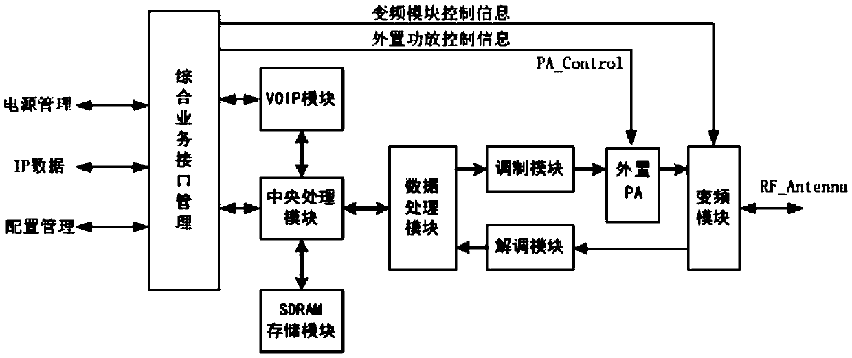
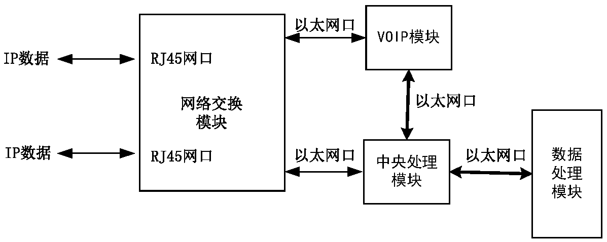
[0025] The present invention provides a dynamic ad hoc network wireless communication device, the device is based on the "CPU and FPGA" architecture design of high-speed data processing, which can improve the data processing speed, such as figure 1 As shown, the present invention includes a central processing module, a data processing module, an SDRAM storage module, an integrated service interface management module, a data processing module, a modulation module, a demodulation module and a frequency conversion module.
[0026] Wherein, central processing module adopts central processing chip to realize, and preferably adopts ColdfireV4 central processing chip in the present invention, and this central processing chip has the configuration of 410MIPS core processing speed, 16KB instruction cache, 16KB data cache and 32KBSRAM. The data processing module is designed with...
PUM
 Abstract
Description
Claims
Application Information