Evaluation equipment for oxide semiconductor thin films

An oxide semiconductor and evaluation device technology, applied in measurement devices, semiconductor/solid-state device testing/measurement, material analysis using microwave means, etc. The effect of reducing setup space

Active Publication Date: 2018-09-04
KOBE STEEL LTD
View PDF8 Cites 0 Cited by
  • Summary
  • Abstract
  • Description
  • Claims
  • Application Information

AI Technical Summary

Problems solved by technology

However, in the contact-type characteristic evaluation method that requires electrode addition, it takes time and cost for electrode addition
In addition, there is a possibility that new defects will be generated in the oxide semiconductor thin film by performing electrode addition

Method used


Image

  • Evaluation equipment for oxide semiconductor thin films
  • Evaluation equipment for oxide semiconductor thin films
  • Evaluation equipment for oxide semiconductor thin films

Examples


Embodiment Construction

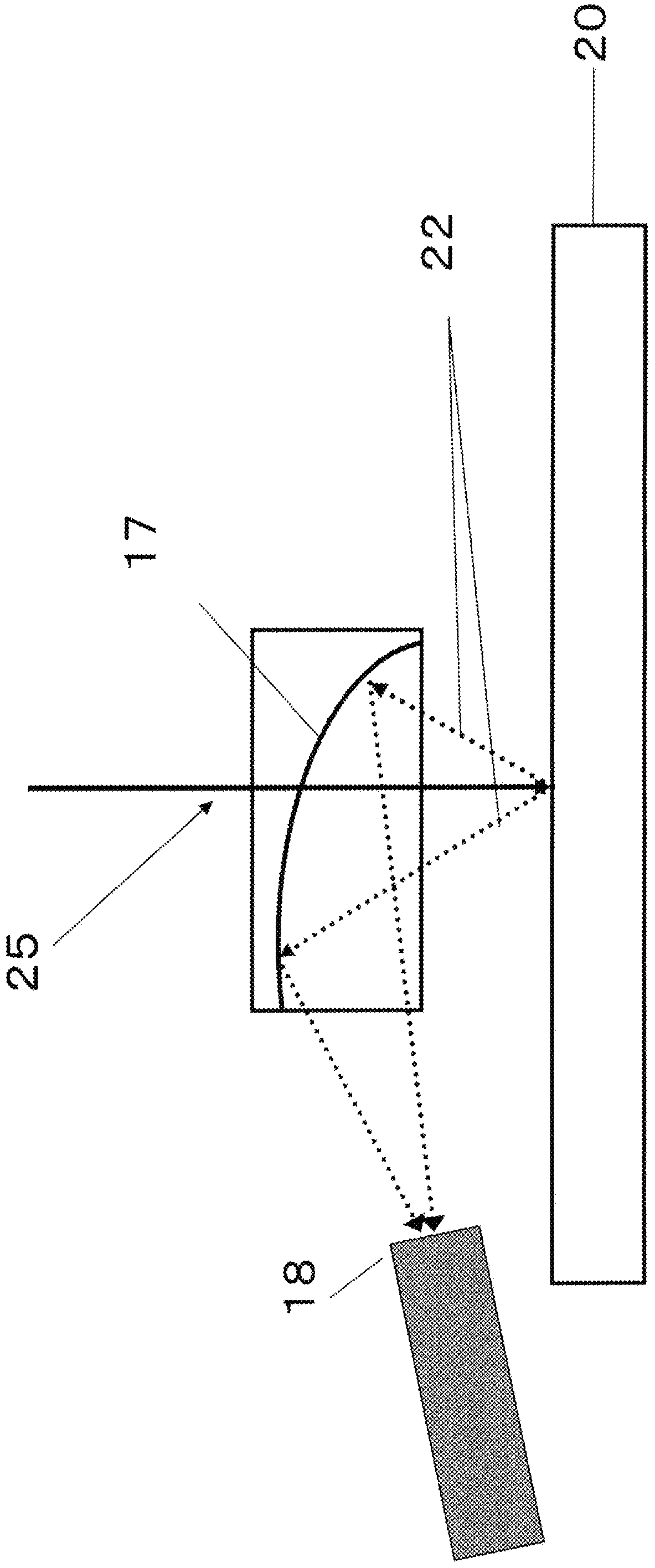
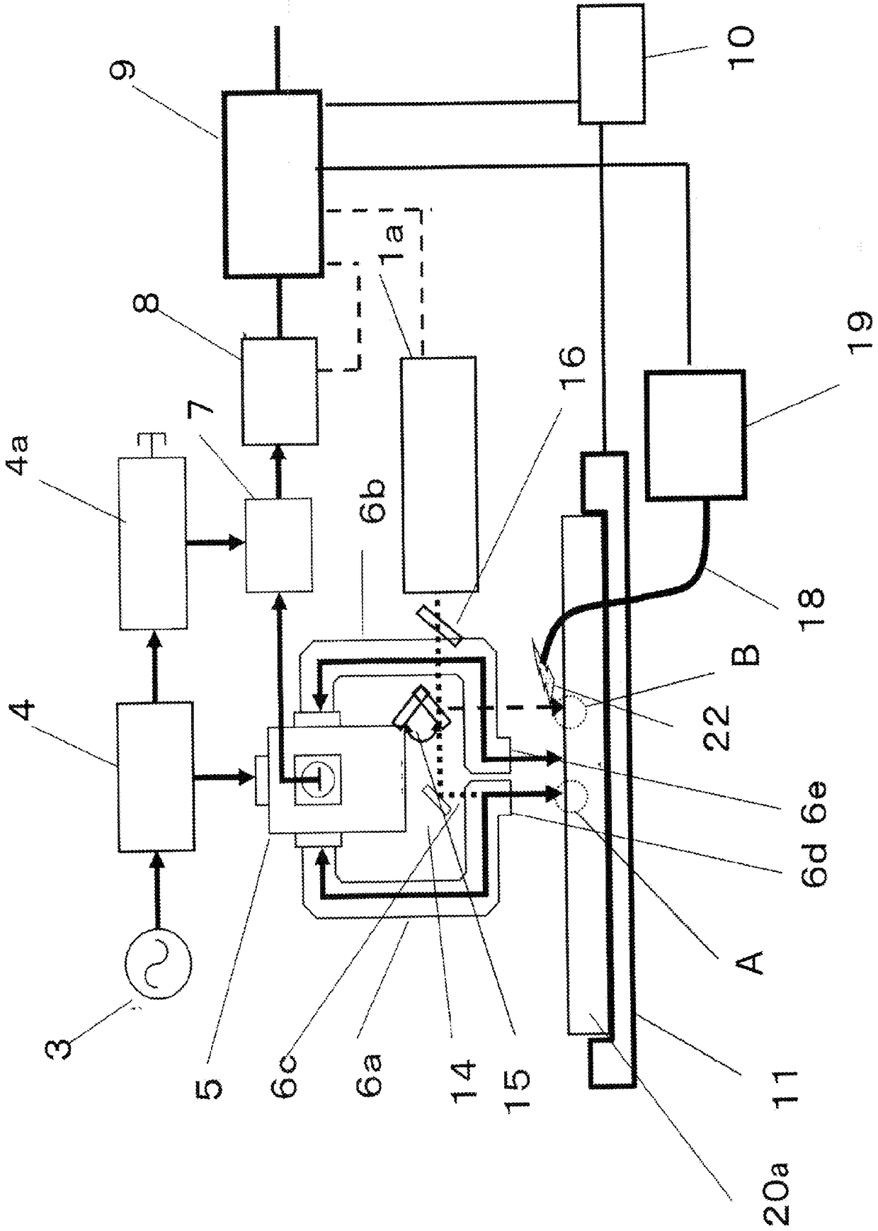
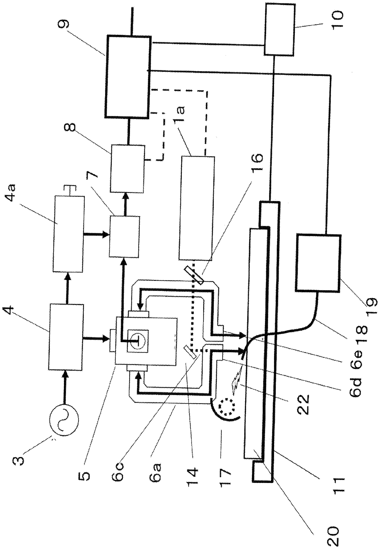
[0031] As already described, the present applicant proposed an evaluation method using a microwave photoconductivity decay method as a technique for evaluating the mobility of an oxide semiconductor thin film. The evaluation method by the microwave photoconductivity attenuation method is a non-contact measurement that does not require electrode addition and can be measured in a short time. Therefore, in the present invention, the known microwave photoconductivity attenuation method is also used. to evaluate.

[0032] On the other hand, since the stress tolerance cannot be evaluated by the previously proposed technique, the inventors of the present invention have intensively discussed the evaluation method of the stress tolerance repeatedly. As a result, it was found that, as an index for easily evaluating (predicting and estimating) the stress resistance of an oxide semiconductor thin film in a non-contact manner, measurement of photoluminescence light excited by irradiating a...


PUM

PropertyMeasurementUnit
thicknessaaaaaaaaaa

Abstract

To provide an evaluation device capable of predicting and estimating the mobility and stress tolerance of an oxide semiconductor thin film by measuring it non-contact, accurately, and simply using the same device. The evaluation device of the present invention includes: a first excitation light irradiation unit that irradiates a measurement site of a sample with first excitation light to generate electron-hole pairs; an electromagnetic wave irradiation unit that irradiates electromagnetic waves; and a reflected electromagnetic wave that detects the intensity of reflected electromagnetic waves. an intensity detection unit; a second excitation light irradiation unit that irradiates the sample with second excitation light to generate photoluminescence light; a luminescence intensity measurement unit that measures the luminescence intensity of the photoluminescence light; and evaluates mobility and An evaluation unit for stress tolerance, wherein the first excitation light irradiation unit and the second excitation light irradiation unit are the same or different excitation light irradiation units.

Description

technical field [0001] The present invention relates to an evaluation device for oxides for semiconductor layers of thin film transistors (TFT: Thin Film Transistor) used in display devices such as liquid crystal displays and organic EL displays (hereinafter referred to as "oxide semiconductor thin films"). In detail, it relates to a device for evaluating the mobility and stress tolerance of an oxide semiconductor thin film in a non-contact type. Background technique [0002] An amorphous (amorphous) oxide semiconductor thin film has higher carrier mobility and a larger optical bandgap than general-purpose amorphous silicon (hereinafter referred to as "a-Si"), and can be formed at a low temperature. Therefore, applications to next-generation displays requiring large-scale, high-resolution, and high-speed drives, and resin substrates with low heat resistance are expected. [0003] Among the oxide semiconductor thin films, for example, In-Ga-Zn-O, In-Ga-Zn- Amorphous oxide s...

Claims


Application Information

Patent Timeline
Patent Type & Authority Patents(China)
IPC IPC(8): H01L21/66G01N21/64
CPCH01L22/12G01N21/6489G01N22/00G01N2201/06113G01N2201/0697
Inventor 林和志岸智弥
Owner KOBE STEEL LTD
Why Eureka
Try Eureka