A kind of chip arrangement resistance vacuum coating method

A technology of vacuum coating and resistance, which is applied in the direction of vacuum evaporation coating, resistors, resistance manufacturing, etc. It can solve the problem that the resistance grooves arranged in the array are easy to be sputtered, and achieve the effect of improving product quality and improving production efficiency

Active Publication Date: 2018-07-20
RALEC TECH KUNSHAN LTD
View PDF4 Cites 0 Cited by
  • Summary
  • Abstract
  • Description
  • Claims
  • Application Information

AI Technical Summary

Problems solved by technology

[0003] Aiming at the deficiencies in the prior art, the purpose of the present invention is to provide a vacuum coating method for wafer array resistors, which can effectively solve the problem that the grooves of array resistors are easily sputtered, so that the end faces of wafer array resistors can be coated with silver for use Vacuum coating technology replaces roll-dipping method to improve product quality and production efficiency

Method used


Image

  • A kind of chip arrangement resistance vacuum coating method
  • A kind of chip arrangement resistance vacuum coating method
  • A kind of chip arrangement resistance vacuum coating method

Examples


Embodiment 1

[0044] Embodiment 1: a kind of wafer arrangement resistance vacuum coating method, it comprises the following steps:

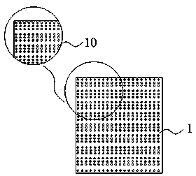
[0045] Substrate preparation: take a substrate 1, a plurality of holes 10 are evenly distributed in a matrix on the substrate 1, wherein every three holes are vertically arranged as a group;

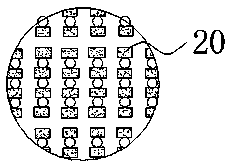
[0046] Step C2: print the conductor 20 on the back side of the substrate, see attached figure 2 ;

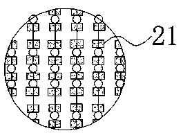
[0047] Step C1: Print conductor 21 on the front side of the substrate, see attached image 3 ;

[0048] Step RS: print resistance 22 on the front side of the substrate, the position of resistance 22 is between two printed conductors adjacent to the front side of the substrate, see Figure 4 ;

[0049] Step G1: After the step RS is finished, print the resistance layer protection layer 23 on the substrate 1, and the resistance layer protection layer 23 covers the resistance 22 printed in the step RS, see Figure 5 ;

[0050] Step LT: laser cutting resistance, adjust r...

Embodiment 2

[0057] Embodiment 2: The difference between this embodiment and Embodiment 1 is that in this embodiment, the printing thickness when printing the conductor in step C2 is 31±10 μm; the printing thickness when printing the conductor in step C1 is 25±10 μm; step RS The printing thickness of the medium resistance is 20±10 μm; the printing thickness of the resistive protective layer in step G1 is 20±10 μm; the thickness of the printed laser protective layer in step G2 is 20±10 μm.

Embodiment 3

[0058] Embodiment 3: The difference between this embodiment and Embodiment 1 is that in this embodiment, during the silver termination process, the impedance of the coating on both sides of each resistance unit: ≦65Ω; during the electroplating process, the plating on the surface of each resistance unit The thickness of the nickel layer is between 5.0-6.0 μm; the thickness of the galvanized layer on the surface of each resistance unit is between 7.0-8.0 μm.


PUM

PropertyMeasurementUnit
thicknessaaaaaaaaaa
thicknessaaaaaaaaaa
thicknessaaaaaaaaaa

Abstract

The invention discloses a chip resistor array vacuum coating method. The chip resistor array vacuum coating method comprises the following steps: substrate preparation: preparing a substrate, wherein a plurality of holes are distributed uniformly in the substrate in an array manner, and every three holes are vertically arranged as one group; step C2, step C1, step RS, step G1, step LT, step G2, stacking, cutting off to obtain grains, electroplating, testing and packaging. By mean of the chip resistor array vacuum coating method, due to improvement of techniques, a problem that grooves of a resistor array are easy to sputter can be effectively solved, so that a vacuum coating technique instead of a rolling-soaking silver coating manner is utilized to perform silver coating on an end face of a chip resistor array, and the quality of products and the production efficiency are improved.

Description

technical field [0001] The invention relates to the field of electronic component production, in particular to a wafer array resistance vacuum coating method. Background technique [0002] In the field of chip resistor production, due to the presence of grooves in the chip array resistors and network resistors, the end-face silver coating generally adopts the end-face silver coating method, that is, use the sponge roller to dip the silver ink evenly, and then turn the sponge roller to apply the silver ink on the resistor. end face of the device. However, this silver coating method needs to rely on manual inspection of the silver coating effect in production. The production efficiency is low, the labor intensity is high, the cost of raw materials is high, it is difficult to control the silver coating effect, and the yield rate is low; and in During the silver coating process, the grooves of the chip array resistors are easy to be coated. Therefore, improving the chip arrang...

Claims


Application Information

Patent Timeline
Patent Type & Authority Patents(China)
IPC IPC(8): H01C17/065H01C17/28C23C14/04
CPCC23C14/04H01C17/06506H01C17/288
Inventor 管春风
Owner RALEC TECH KUNSHAN LTD
Why Eureka
Try Eureka