Flexible display device and manufacturing method of the same

A flexible display device and manufacturing method technology, applied in semiconductor/solid-state device manufacturing, semiconductor devices, electrical components, etc., can solve the problem of reducing packaging performance, brittleness and cracking of inorganic film layers, bending, curling and even folding of flexible OLED devices, etc. problems, to prevent the intrusion of water vapor and oxygen, reduce stress build-up, and inhibit fractures and cracks

Inactive Publication Date: 2016-05-04
SHANGHAI TIANMA MICRO ELECTRONICS CO LTD +1
View PDF4 Cites 57 Cited by
  • Summary
  • Abstract
  • Description
  • Claims
  • Application Information

AI Technical Summary

Problems solved by technology

Although such a packaging structure has good water and oxygen barrier properties and can ensure the service life of the OLED, the flexible OLED device will be bent, curled or even folded during use.
During the bending process, the s

Method used


Image

  • Flexible display device and manufacturing method of the same
  • Flexible display device and manufacturing method of the same
  • Flexible display device and manufacturing method of the same

Examples


Embodiment 1

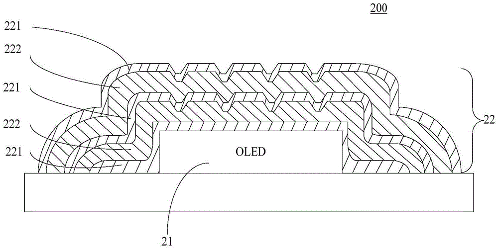
[0045] Please refer to figure 2 , which shows a schematic structural view of an embodiment of the flexible display device of the present application.

[0046] Such as figure 2 As shown, the flexible display device 200 of this embodiment includes a light emitting device 21 and an encapsulation layer 22 for encapsulating the light emitting device 21 . The encapsulation layer 22 includes at least one organic film layer 222 and at least one inorganic film layer 221 stacked together.

[0047] The organic film layer 222 may have one layer or multiple layers; the organic film layer 222 may directly cover the light emitting device 21 or not directly wrap the light emitting device 21 .

[0048] here, despite figure 2 3 schematically shows 3 layers of inorganic film layers 221 and 2 layers of organic film layers 221 . However, figure 2 The number of inorganic film layers and the number of organic film layers in are only illustrative. In practice, the number of inorganic film l...

Embodiment 2

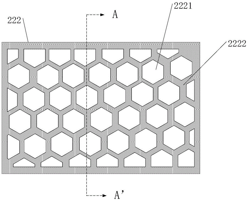
[0062] In this embodiment, the same structure as the above embodiment will not be repeated here, the difference is that the area of ​​the pattern unit in the organic film layer can be changed to adjust the bending resistance of the inorganic layer. Optionally, the area of ​​each graphic unit can be 10 3 Square micron ~ 10 5 square micron.

[0063] Within this area range, the size of the graphics unit is equivalent to the area of ​​one pixel of the display device. E.g Figure 6A It is a top view of the encapsulation layer of the flexible display device in this embodiment, Figure 6B For this example Figure 6A Section view along AA'. refer to Figure 6A with Figure 6B , one pixel of the flexible display device corresponds to one graphic unit of the organic film layer 222 . That is to say, the area of ​​the graphics unit 2221 can be set as the area of ​​one pixel 2011 in the pixel layer 201 . from Figure 6B It can be seen from the figure that the top of a pixel 2011 ...

Embodiment 3

[0075] This embodiment provides a method for manufacturing a flexible display device,

[0076] Such as Figure 8 As shown, it is a schematic flow chart of the manufacturing method of the flexible display device provided by the embodiment of the present application

[0077] A method for manufacturing a flexible display device includes the following steps:

[0078] Step 801, forming a light emitting device.

[0079] In some optional implementation manners of this embodiment, the light emitting device may be formed according to any light emitting device forming process.

[0080] Step 802, forming an encapsulation layer encapsulating the light emitting device.

[0081] In some optional implementation manners, the step of forming an encapsulation layer encapsulating the light-emitting device may further include, for example:

[0082] Step 8021, forming at least one organic film layer, the organic film layer includes graphic units and non-graphic units separating the graphic uni...


PUM

PropertyMeasurementUnit
Thicknessaaaaaaaaaa
Thicknessaaaaaaaaaa
Thicknessaaaaaaaaaa

Abstract

The invention discloses a flexible display device and a manufacturing method of the same. A specific embodiment of the flexible display device includes a luminescent device and a packaging layer used for packaging the luminescent device, the packaging layer includes at least one organic membrane layer and at least one inorganic membrane layer which are superposed, wherein the organic membrane layer includes a plurality of pattern units and non-pattern units used for separating the plurality of the pattern units, the thickness of the pattern units and that of the non-pattern units are not the same, and the inorganic membrane layers cover the pattern units and the non-pattern units. According to the flexible display device provided by the invention, the organic membrane layers are divided into the pattern units and the non-pattern units, and the thickness of the pattern units and that of the non-pattern units are different, thereby enabling the inorganic membrane layers uniformly covering the organic membrane layers to become uneven. Thus water steam and oxygen can be prevented from immerging into the luminescent device, and cracks of the inorganic membrane layers generated due to stress concentration can also be prevented.

Description

technical field [0001] The present application relates to the field of display technology, in particular to the field of flexible display technology, and in particular to a flexible display device and a method for manufacturing the flexible display device. Background technique [0002] With the rapid growth of demand for portable mobile devices and wearable display products, flexible display technology has made great progress in recent years. In the display technology that can realize flexible display, OLED (Organic Light Emitting Display, organic light-emitting diode display) is considered as a flexible display because of its excellent properties such as anti-bending, fast response, wide viewing angle, light weight, low power consumption, and high brightness. One of the most promising technologies in technology. [0003] The OLED device itself is very sensitive to water vapor and oxygen, and OLEDs exposed to water vapor and oxygen will have poor working stability and reduc...

Claims


Application Information

Patent Timeline
IPC IPC(8): H01L51/52H01L51/00H01L51/56
CPCH10K71/20H10K50/8445
Inventor 蔡雨
Owner SHANGHAI TIANMA MICRO ELECTRONICS CO LTD
Why Eureka
Try Eureka