Substrate of anti-CAF (Conductive Anodic Filament) printed circuit board and manufacturing method thereof

A technology for printed circuit boards and manufacturing methods, which is applied in the direction of printed circuit manufacturing, printed circuits, printed circuit components, etc., and can solve problems such as product short circuit failure, glass fiber layer breakage or poor bonding

Active Publication Date: 2016-05-04
KUSN HULI MICROELECTRONICS
View PDF6 Cites 3 Cited by
  • Summary
  • Abstract
  • Description
  • Claims
  • Application Information

AI Technical Summary

Problems solved by technology

[0003] The production process may cause a well-known failure phenomenon called glass fiber metal ion migration (ConductiveAnodicFilament/CAF) due to the fracture or poor bonding of the glass fiber layer. This refers to the phenomenon

Method used


Image

  • Substrate of anti-CAF (Conductive Anodic Filament) printed circuit board and manufacturing method thereof
  • Substrate of anti-CAF (Conductive Anodic Filament) printed circuit board and manufacturing method thereof
  • Substrate of anti-CAF (Conductive Anodic Filament) printed circuit board and manufacturing method thereof

Examples


Embodiment Construction

[0025] The present invention will be specifically introduced below in conjunction with the accompanying drawings and specific embodiments.

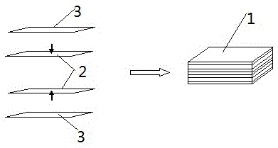
[0026] The substrate 1 of the anti-CAF printed circuit board, the prepreg 2, and the metal layer 3 covering the upper and lower positions of the prepreg 2, as a preference, the metal layer 3 is copper foil; the prepreg 2 is a fragmented prepreg 2. Fragmented prepreg 2 is at least one layer. Fragmented prepreg 2 consists of broken glass yarn and epoxy resin wrapping the broken glass yarn. The length of the broken glass yarn is less than the hole-to-hole gap distance on the printed circuit board. Fragmented prepreg 2 reduces the influence of the spinning effect of warp and weft yarns in the glass cloth, so that the size of the substrate can expand and shrink more uniformly, because the more uniform the glass plus resin structure, the more it can make the traditional PCB production process such as drilling, plated through The hole process ...


PUM


Abstract

The invention discloses a substrate of an anti-CAF (Conductive Anodic Filament) printed circuit board and a manufacturing method thereof; the substrate comprises a prepreg and metal layers, wherein the metal layers cover on upper and lower positions of the prepreg; the prepreg is the fragmented prepreg; and the manufacturing method for the substrate of the anti-CAF printed circuit board comprises the following steps: step 1, manufacturing the prepreg; step 2, crushing the prepreg; and step 3, manufacturing the substrate. According to the substrate of the anti-CAF printed circuit board and the manufacturing method thereof disclosed by the invention, by adopting a treatment manner of crushing the prepreg, the spinning effect influence of warp and weft yarns in glass fiber cloth can be reduced, so that the dimension swelling and contracting of a base material can be more uniform, and the opportunity for glass fiber diffusion coating is reduced.

Description

technical field [0001] It relates to a printed circuit board and a manufacturing method, in particular to a substrate of a printed circuit board and a manufacturing method thereof. Background technique [0002] The production process of Printed circuit board (PCB) requires drilling and copper plating to connect the inner and outer layers to form a multi-layer board. This process requires cutting or drilling several layers of glass fiber reinforcement layers and the glass fiber layer It is made by using glass fiber to form a thin layer by spinning and weaving, and then bonding it with resin. [0003] The production process may cause a well-known failure phenomenon called glass fiber metal ion migration (ConductiveAnodicFilament / CAF) due to the fracture or poor bonding of the glass fiber layer. This refers to the phenomenon of ion migration of copper ions under electrical bias, making Serious short-circuit failure occurs in the product. This phenomenon may occur in hollow gla...

Claims


Application Information

Patent Timeline
IPC IPC(8): H05K1/02H05K3/38
CPCH05K1/0366H05K3/381H05K2203/06
Inventor 乔迪克森
Owner KUSN HULI MICROELECTRONICS
Why Eureka
Try Eureka