Method for fabricating line between two bonding pads of PCB

A line and pad technology, applied in the field of circuit board production, can solve problems such as poor pad welding, line offset, incompleteness, etc., and achieve the effect of clear lines and guaranteed quality

Active Publication Date: 2016-05-04
大连崇达电子有限公司
View PDF4 Cites 4 Cited by
  • Summary
  • Abstract
  • Description
  • Claims
  • Application Information

AI Technical Summary

Problems solved by technology

[0003] The present invention aims at the prior art to make lines between two pads with a distance of less than 0.336mm, which will easily cause the lines to shift to the pads and the ink will not be placed in the line area, resulti

Method used


Image

  • Method for fabricating line between two bonding pads of PCB
  • Method for fabricating line between two bonding pads of PCB
  • Method for fabricating line between two bonding pads of PCB

Examples


Embodiment

[0019] This embodiment provides a method for manufacturing a PCB, especially a method for making lines between two pads of the PCB. Specific steps are as follows:

[0020] (1) multilayer board

[0021] According to the existing technology, the substrate is made into a production board with an outer circuit by sequentially going through material cutting→negative film process to make inner layer circuit→pressing→drilling→immersion copper→full board electroplating→positive film process to make outer layer circuit, Called multi-layer board. The multi-layer board includes at least two pads, and the distance between the two pads is 0.14mm, and a line with a line width of 0.07mm needs to be formed between the two pads in the post-production process.

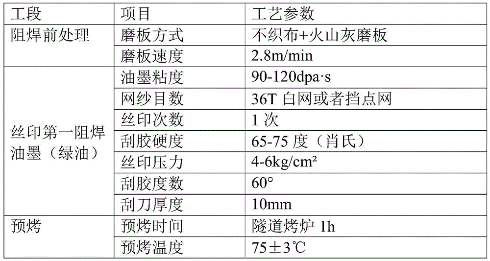
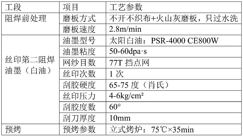
[0022] (2) One-time screen printing solder resist ink

[0023] The first solder resist ink is screen-printed on the multilayer board through the first screen printing screen, and then the first solder resist ink on the multilayer boa...


PUM


Abstract

The invention relates to the technical field of production of circuit boards, in particular to a method for fabricating a line between two bonding pads of a PCB. The line is fabricated between the two bonding pads in manners of screen printing, exposure and development. The minimal distance between the line and each bonding pad can be 0.035mm according to the exposure accuracy of the prior art; and the minimal width of the line can be 0.07mm. Therefore, the method provided by the invention can fabricate the line between the bonding pads between which the space is equal to or greater than 0.14mm; and the condition that the line is clear and intact and does not deviate to the bonding pads can be ensured, so that the quality of a PCB product is ensured. The problem that the line cannot be fabricated between the two bonding pads between which the space is smaller than 0.336mm under the premise of ensuring the quality in the prior art is solved.

Description

technical field [0001] The invention relates to the technical field of circuit board production, in particular to a method for making lines between two pads of a PCB. Background technique [0002] PCB (Printed Circuit Board), the Chinese name is printed circuit board, also known as printed circuit board, is an important electronic component, a support for electronic components, and a carrier for electrical connections of electronic components. With the diversified development of electronic products, the design of PCB also tends to be diversified. In order to meet some special functional requirements, it is necessary to make lines between the two pads of the PCB. The existing technology uses silk screen characters to make lines between the two pads, and according to the ability of the existing silk screen characters, the minimum distance between the lines and the pads is 0.13mm, and the LDS ultraviolet laser screen plate-making machine can print out the light. The minimum l...

Claims


Application Information

Patent Timeline
IPC IPC(8): H05K3/00H05K3/28
CPCH05K3/0073H05K3/28H05K2203/0537H05K2203/1476
Inventor 罗家伟张庭生胡志勇钟宇玲
Owner 大连崇达电子有限公司
Why Eureka
Try Eureka