Fabrication method of lateral high voltage semiconductor device

A technology of lateral high voltage and manufacturing method, applied in semiconductor/solid-state device manufacturing, electrical components, circuits, etc., can solve problems such as increased on-resistance, and achieve the effect of avoiding breakdown voltage and on-resistance

Active Publication Date: 2019-03-05
FOUNDER MICROELECTRONICS INT
View PDF6 Cites 0 Cited by
  • Summary
  • Abstract
  • Description
  • Claims
  • Application Information

AI Technical Summary

Problems solved by technology

[0005] The invention provides a method for manufacturing a lateral high-voltage semiconductor device to solve the problem in the prior art that when the breakdown voltage of a lateral high-voltage semiconductor device is increased, the on-resistance also increases

Method used


Image

  • Fabrication method of lateral high voltage semiconductor device
  • Fabrication method of lateral high voltage semiconductor device
  • Fabrication method of lateral high voltage semiconductor device

Examples


Embodiment Construction

[0031] This embodiment provides a method for manufacturing a lateral high voltage semiconductor device. like Figures 2A-2H As shown, is a schematic flow chart of the method for fabricating a lateral high-voltage semiconductor device according to this embodiment.

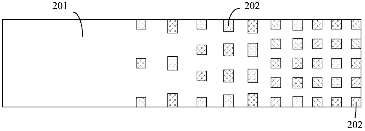
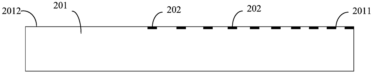
[0032] like Figure 2A As shown, it is a schematic top view of forming each first ion-implanted doped region on the substrate; as Figure 2B Shown is a schematic cross-sectional view of forming each first ion-implanted doped region on the substrate.

[0033] In this embodiment, on the surface layer of the substrate 201 of the first conductivity type, each first ion-implanted doped region 202 of the second conductivity type is formed, and the distribution density of the first ion-implanted doped regions 202 is changed from the high-voltage The terminal 2011 gradually decreases toward the low-voltage terminal 2012 of the lateral high-voltage semiconductor device.

[0034] Both the first conductivity type and the s...


PUM


Abstract

The invention provides a manufacturing method of a transverse high-voltage semiconductor device. The manufacturing method comprises the steps of forming second-conductive-type first ion implantation doped regions on the surface of a first-conductive-type substrate, wherein the distribution density of the first ion implantation doped region gradually reduces in a direction from the high-voltage end of the transverse high-voltage semiconductor device to the low-voltage end of the transverse high-voltage semiconductor device; performing first high-temperature treatment on the substrate so that the first ion implantation doped regions form a first diffusion region; forming an epitaxial layer on the substrate; and forming a second-conductive-type second diffusion region and a first-conductive-type third diffusion region on the surface layer of the epitaxial layer, wherein the third diffusion region is arranged at the low-voltage end, the second diffusion region covers the first diffusion region and extends from one side, which is next to the high-voltage end, of the third diffusion region to the high-voltage end, and the second conductive type is opposite to the first conductive type. The manufacturing method of the transverse high-voltage semiconductor device according to the invention prevents contradiction between breakdown voltage and on-resistance as possible.

Description

technical field [0001] The invention relates to semiconductor device technology, in particular to a method for manufacturing a lateral high-voltage semiconductor device. Background technique [0002] Lateral high-voltage semiconductor devices are commonly used in power integrated circuits, and their high-voltage terminals can withstand high potentials. The maximum voltage that the high-voltage terminals can withstand is called "breakdown voltage". When a lateral high-voltage semiconductor device is turned on, the impedance between the high-voltage terminal and the low-voltage terminal is called "on-resistance". For the same lateral high-voltage semiconductor device, the larger the breakdown voltage, the better, and the smaller the on-resistance. [0003] The lateral high-voltage semiconductor device includes a lateral double-diffused metal oxide transistor (Laterally Diffused Metal Oxide Semiconductor, LDMOS), a lateral insulated gate bipolar transistor (Lateral Insulated Ga...

Claims


Application Information

Patent Timeline
Patent Type & Authority Patents(China)
IPC IPC(8): H01L21/265
Inventor 潘光燃石金成文燕王焜高振杰
Owner FOUNDER MICROELECTRONICS INT
Why Eureka
Try Eureka