Formation method of metal interconnection structure

A metal interconnection structure, metal layer technology, applied in electrical components, semiconductor/solid-state device manufacturing, circuits, etc., can solve problems such as electromigration failure, high resistance, disconnection, etc., to improve performance and reduce defects that form voids Effect

Inactive Publication Date: 2016-05-11
SEMICON MFG INT (SHANGHAI) CORP
View PDF3 Cites 5 Cited by
  • Summary
  • Abstract
  • Description
  • Claims
  • Application Information

AI Technical Summary

Problems solved by technology

[0007] However, in the actual process of metal interconnect structure preparation, combined with reference figure 2 , taking the first plug 121 as an example, when the conductive material 122 is filled into the first trench 12 of the first dielectric layer 11, a void 15 will be formed in the conductive material in the first trench 12, The void 15 will lead to defects such as disconnection of the subsequently formed first conductive plug 121, high resistance, and electromigration failure (the above-mentioned defects also exist in the interconnection line), thereby reducing the performance of the semiconductor device.

Method used


Image

  • Formation method of metal interconnection structure
  • Formation method of metal interconnection structure
  • Formation method of metal interconnection structure

Examples


Embodiment Construction

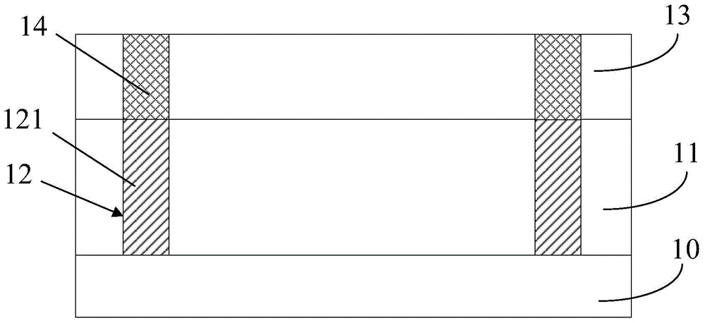
[0043] As mentioned in the background art, using the existing technology, during the process of forming the metal interconnection structure in the dielectric layer, a larger volume of voids will be formed in the conductive plugs and interconnection lines, thereby reducing the metal interconnection structure. performance. Especially as the process node of the integrated circuit continues to decrease, the aspect ratio of the trench formed in the dielectric layer for forming the metal interconnection structure increases, so that the gap formed in the metal interconnection structure takes up the space between the conductive plug and the interconnection structure. The space ratio of the wiring is gradually increasing, which has a more serious impact on the performance of the conductive plug and the interconnection line. Analyze the cause of the gap:

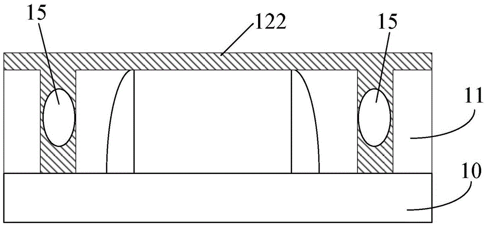
[0044] In the existing technology, copper is mostly used as the material of the metal interconnection structure, refer to image 3...


PUM

PropertyMeasurementUnit
thicknessaaaaaaaaaa
thicknessaaaaaaaaaa
thicknessaaaaaaaaaa

Abstract

The invention provides a formation method of a metal interconnection structure. The method comprises that a metal seed crystal layer is formed at the surface of a semiconductor substrate and in grooves of the semiconductor substrate, and then a shield layer is formed at the surface of the metal seed crystal layer; and the shield layer at the bottom of the grooves is removed to expose the metal seed crystal layer at the bottom of the grooves, and the shield layer which covers the sidewalls of the grooves is reserved. In the subsequent process that a metal layer is formed on the metal seed crystal layer, the metal layer cannot be formed at the sidewalls of the grooves due to that the sidewalls of the grooves are covered with the shield layer, and the metal layer can be only formed from bottom to top gradually on the metal seed crystal layer, which is exposed at the bottom of the grooves, till the grooves are filled; the defect that gaps are formed in the metal layer in the grooves due to the fact that openings of the grooves are closed too early when the grooves are not full of metal layer; and further, the performance of the metal interconnection structure formed in the grooves subsequently and the performance of a semiconductor device formed subsequently are improved.

Description

technical field [0001] The invention relates to the field of semiconductor manufacturing, in particular to a method for forming a metal interconnection structure. Background technique [0002] With the rapid development of integrated circuit (abbreviated as IC) manufacturing technology, the process nodes of traditional integrated circuits are gradually reduced, and the size of integrated circuit devices is continuously reduced. On a wafer, the number of semiconductor components is continuously increased. Processes are constantly being innovated to improve the performance of integrated circuit devices. [0003] For example, in order to meet the requirements of increasing the number of semiconductor elements, semiconductor elements with a multi-layer structure are usually formed on a wafer, and the semiconductor elements of adjacent layers are electrically connected through a metal interconnection structure, thereby increasing the number of semiconductor elements on a chip wit...

Claims


Application Information

Patent Timeline
Patent Type & Authority Applications(China)
IPC IPC(8): H01L21/768
Inventor 刘继全
Owner SEMICON MFG INT (SHANGHAI) CORP
Why Eureka
Try Eureka