A method for forming a semiconductor structure

A semiconductor and metal structure technology, applied in semiconductor/solid-state device manufacturing, electrical components, circuits, etc., can solve problems such as performance and reliability to be improved, and achieve the effect of reducing the risk of short circuit, reducing damage, and improving density

Pending Publication Date: 2022-02-18
SEMICON MFG INT (SHANGHAI) CORP +1
View PDF0 Cites 0 Cited by
  • Summary
  • Abstract
  • Description
  • Claims
  • Application Information

AI Technical Summary

Problems solved by technology

[0004] However, the performance and reliability of existing semiconductor devices still need to be improved

Method used


Image

  • A method for forming a semiconductor structure
  • A method for forming a semiconductor structure
  • A method for forming a semiconductor structure

Examples


Embodiment Construction

[0032] As mentioned in the background, the performance and reliability of semiconductor structures still needs to be improved. The reasons why the performance and reliability of the semiconductor structure still need to be improved will be described in detail below with reference to the accompanying drawings.

[0033] Figure 1 to Figure 3 It is a schematic cross-sectional structure diagram of the formation process of a semiconductor structure.

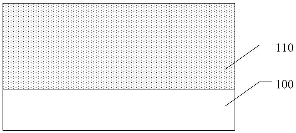
[0034] Please refer to figure 1 , providing a substrate (not shown), the substrate has a metal structure 100 inside, and the metal structure 100 is exposed on the surface of the substrate; a dielectric structure 110 is formed on the surface of the metal structure 100 .

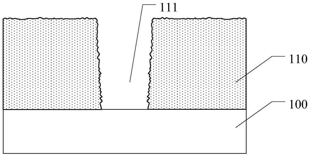
[0035] Please refer to figure 2 , forming a plug mask structure (not shown) on the surface of the dielectric structure 110; using the plug mask structure as a mask, etching the dielectric structure 110 until the surface of the metal structure 100 is exposed, formi...


PUM


Abstract

A method for forming a semiconductor structure comprises the steps of providing a substrate, where a metal structure is arranged in the substrate, and the metal structure is exposed out of the surface of the substrate; forming a dielectric structure on the surface of the metal structure; forming an opening penetrating through the dielectric structure in the dielectric structure; after the opening is formed, performing densification treatment on the side wall surface of the opening and the surface of the dielectric structure; and after the densification treatment, forming an interconnection structure in the opening by adopting a selective metal growth process. Therefore, the performance and the reliability of the semiconductor device are improved.

Description

technical field [0001] The invention relates to the technical field of semiconductor manufacturing, in particular to a method for forming a semiconductor structure. Background technique [0002] At present, in the semiconductor manufacturing process, an etching process is used to form a through hole in the dielectric layer, and then a seed layer is formed on the side wall and bottom of the through hole, and a conductive material is grown on the surface of the seed layer to form an electrical connection structure, so as to realize semiconductor. Electrical connection between devices is a widely used process. However, since the seed layer is formed on the side wall and the bottom surface of the through hole, when the conductive material is grown, the top of the through hole is likely to be closed before the bottom of the through hole is not completely filled with the conductive material, resulting in a void in the electrical connection structure. As a result, the parasitic re...

Claims


Application Information

Patent Timeline
Patent Type & Authority Applications(China)
IPC IPC(8): H01L21/768
CPCH01L21/76814H01L21/76826H01L21/76822H01L21/76834
Inventor 陈建王胜王彦张海洋
Owner SEMICON MFG INT (SHANGHAI) CORP
Why Eureka
Try Eureka