An embedded flash memory, preparation method thereof, and electronic device

An electronic device and embedded technology, applied in circuits, electrical components, electrical solid devices, etc., can solve the problems of holes and holes generated by depositing floating gates, and achieve the effect of good outline, avoidance of holes, and good process window.

Active Publication Date: 2019-05-17
SEMICON MFG INT (SHANGHAI) CORP
View PDF4 Cites 0 Cited by
  • Summary
  • Abstract
  • Description
  • Claims
  • Application Information

AI Technical Summary

Problems solved by technology

[0006] There is the following contradiction in the filling of the logic process and the flash memory process. When the critical dimension of the active region is large, the critical dimension of the shallow trench isolation structure is small and has a large aspect ratio. The process creates holes in the shallow trench isolation oxide, such as Figure 2a and 2b As shown in A; but when the critical dimension of the active region is small, forming a floating gate structure on the active region will lead to holes in the process of depositing the floating gate, such as Figure 2b Shown in B

Method used


Image

  • An embedded flash memory, preparation method thereof, and electronic device
  • An embedded flash memory, preparation method thereof, and electronic device
  • An embedded flash memory, preparation method thereof, and electronic device

Examples


preparation example Construction

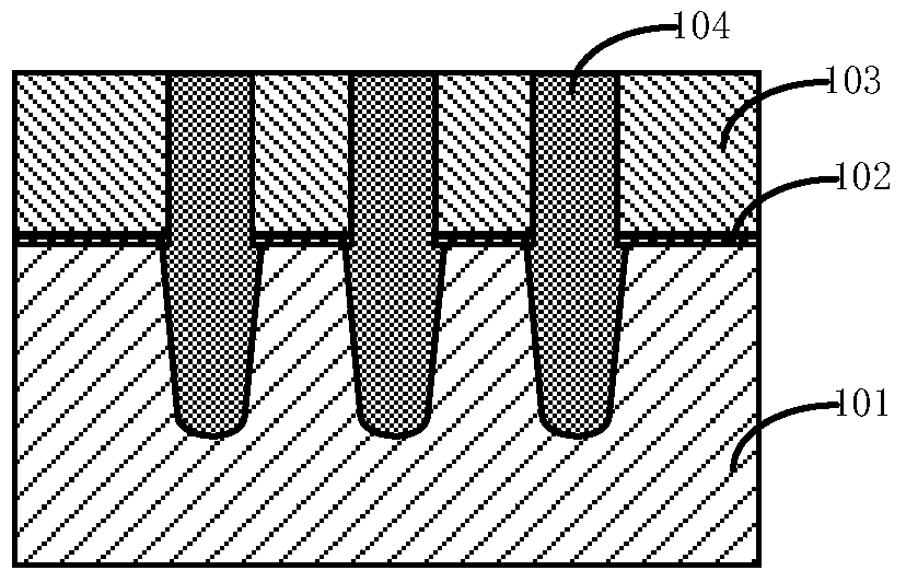
[0053] The preparation method of the embedded flash memory described in the prior art is as Figures 1a-1g As shown, first as Figure 1a As shown, a semiconductor substrate 101 is provided on which an oxide layer 102 and a nitride layer 103 are formed and patterned to form shallow trenches in the oxide layer 102 and the nitride layer 103 , choose shallow trench oxide 104 to fill the shallow trench, and obtain the following Figure 1a pattern shown.

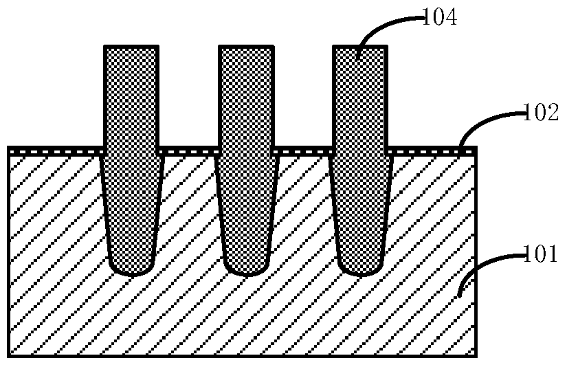
[0054] Then, the nitride layer 103 is removed to obtain Figure 1b structure shown.

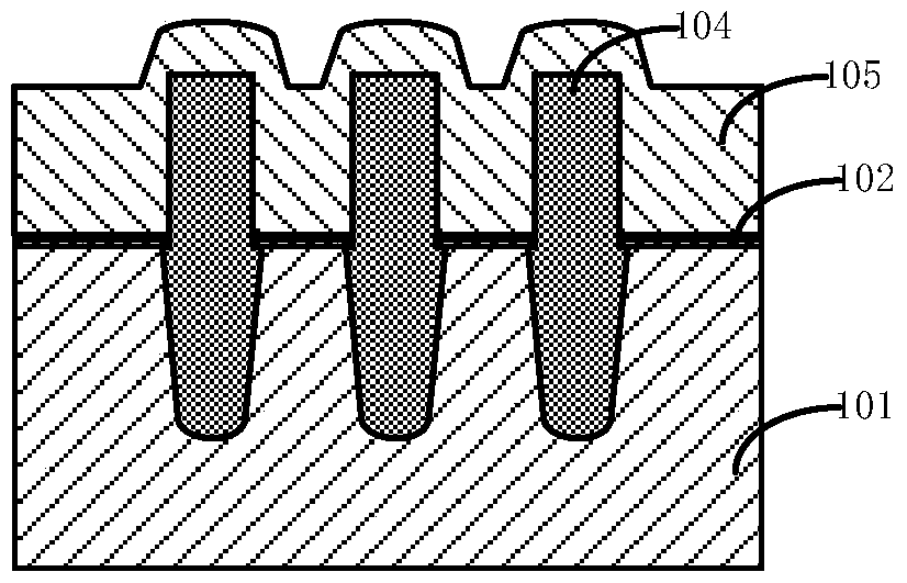
[0055] Next, a floating gate material layer 105 is deposited to cover the oxide layer 102 and the shallow trench oxide 104, to obtain the following Figure 1c structure shown.

[0056] planarizing the floating gate material layer 105 and the shallow trench oxide 104 to a smaller thickness, such as Figure 1d shown.

[0057] Etching back the shallow trench oxide 104 to the oxide layer 102 to form openings in the floating gate material layer...

Embodiment 1

[0062] Step 201 is executed to provide a substrate 201 in which a shallow trench isolation oxide 204 is formed.

[0063] Specifically, such as Figure 3a As shown, the base 201 includes at least a semiconductor substrate, and the semiconductor substrate can be at least one of the materials mentioned below: silicon, silicon-on-insulator (SOI), silicon-on-insulator (SSOI), stack-on-insulator Silicon germanium (S-SiGeOI), silicon germanium on insulator (SiGeOI) and germanium on insulator (GeOI), etc.

[0064] An oxide layer 202 and a nitride layer 203 are sequentially formed on a semiconductor substrate. The oxide layer 202 can be obtained by a high temperature oxidation method, and its thickness can be 100-200 angstroms. The oxide layer 202 may serve as an isolation layer to protect the semiconductor substrate from damage and contamination.

[0065] The nitride layer 203 may be formed by chemical vapor deposition (CVD), physical vapor deposition (PVD) or atomic layer depositi...

Embodiment 2

[0112] The present invention also provides an embedded flash memory, comprising:

[0113] base;

[0114] a shallow trench isolation structure, the bottom of which is embedded in the substrate;

[0115] active regions located in the substrate and isolated from each other by the shallow trench isolation structure;

[0116] T-shaped floating gates are arranged at intervals on the active region, and the horizontal part of the T-shaped floating gate covers part of the top of the shallow trench isolation structure.

[0117] Wherein, the critical dimension at the top of the T-shaped floating gate is 60-110 nm, and the critical dimension at the bottom is 50-75 nm.

[0118] The thickness of the shallow trench isolation structure is 100-1000 angstroms.

[0119] The thickness of the vertical part of the T-shaped floating gate is 60-300 angstroms.

[0120] The embedded flash memory further includes:

[0121] an isolation layer located above the T-shaped floating gate;

[0122] The c...


PUM

PropertyMeasurementUnit
thicknessaaaaaaaaaa
thicknessaaaaaaaaaa

Abstract

The invention relates to an embedded flash memory, a preparation method thereof, and an electronic device. The method comprises that a substrate is provided, an active region isolated by a shallow trench isolation (STI) oxide is formed in the substrate, and the top of the STI oxide is higher than the surface of the substrate; a floating gate material layer is deposited to cover the active region and the STI oxide; the floating gate material layer is flattened to expose the surface of the STI oxide; the floating gate material layer is etched back to reduce the thickness of the floating gate material layer and expose the STI oxide of certain height; the exposed STI oxide is etched back to reduce the key size of the exposed STI oxide; the floating gate material layer is re-deposited till the top of the STI oxide to surround the STI oxide and flatten the floating material layer; and the part whose key size is reduced of the STI oxide is removed to form a T-shaped floating gate on the active region.

Description

technical field [0001] The invention relates to the technical field of semiconductor manufacturing, in particular to an embedded flash memory, a preparation method thereof, and an electronic device. Background technique [0002] In the current semiconductor industry, integrated circuit products can be mainly divided into three types: logic, memory and analog circuits, among which memory devices account for a considerable proportion of integrated circuit products. Among storage devices, the development of flash memory (flash memory for short) is particularly rapid in recent years. Its main feature is that it can keep stored information for a long time without power on, and has many advantages such as high integration, fast access speed, easy erasure and rewriting, etc. The field has been widely used. [0003] With the development of semiconductor technology, storage devices are more widely used, and the storage device and other device regions need to be formed on a chip at ...

Claims


Application Information

Patent Timeline
Patent Type & Authority Patents(China)
IPC IPC(8): H01L27/11524H01L27/11521
Inventor 王新鹏
Owner SEMICON MFG INT (SHANGHAI) CORP
Why Eureka
Try Eureka