Laser unsealing method

A laser and laser ablation technology, applied in laser welding equipment, electrical components, circuits, etc., can solve problems such as copper bonding corrosion and broken wires, damage to microwave device chips, uncontrolled unsealing process, etc., to avoid structural damage , Improve the accuracy of unsealing and improve the success rate

Active Publication Date: 2016-05-25
CASIC DEFENSE TECH RES & TEST CENT
View PDF7 Cites 33 Cited by
  • Summary
  • Abstract
  • Description
  • Claims
  • Application Information

AI Technical Summary

Problems solved by technology

[0010] However, since the working mode of the acid unsealing machine is to use high-pressure nitrogen as a power source to push the acid to impact the surface of the sample, the unsealing area after the etching of the plastic-encapsulated device unsealing machine is often larger than the predetermined unsealing area (ie, the diffusivity of acid unsealing), which is not conducive to Precise control of Kaifeng area
At the same time, the unsealing process is uncontrolled. The technicians set the temperature of the acid, the flow rate of the acid and the etching time based on experience. The process state of the sample cannot be observed during the unsealing process. The unsealing process is uncontrolled and cannot be intuitively and effectively Control the corrosion of samples in acid solution
[0011] Due to the above problems, it is inevitable that the copper bonding will be corroded and broken, the chips of GaAs and other microwave devices will be damaged, and the bottom printed board of the multi-chip device will be corroded, which will cause the sample to lose its original electrical characteristics or introduce secondary defects.

Method used


Image

  • Laser unsealing method
  • Laser unsealing method
  • Laser unsealing method

Examples


Embodiment 1

[0049] As an embodiment of the present invention, taking LT Company's LTM series DC / DC and other hybrid plastic-encapsulated circuits (conventional plastic-encapsulated devices) as an example, the laser unsealing method includes the following steps:

[0050] 1) Before unsealing, the position and depth of each component and chip inside the plastic-encapsulated device are positioned by micro-focus X-rays to obtain the size, position and depth information of each component and chip inside the device. In general, unpacking only needs to expose the internal chips, inductors and resistors, so it is only necessary to remove the molding materials on the surface of these components and chips.

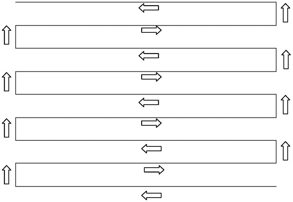
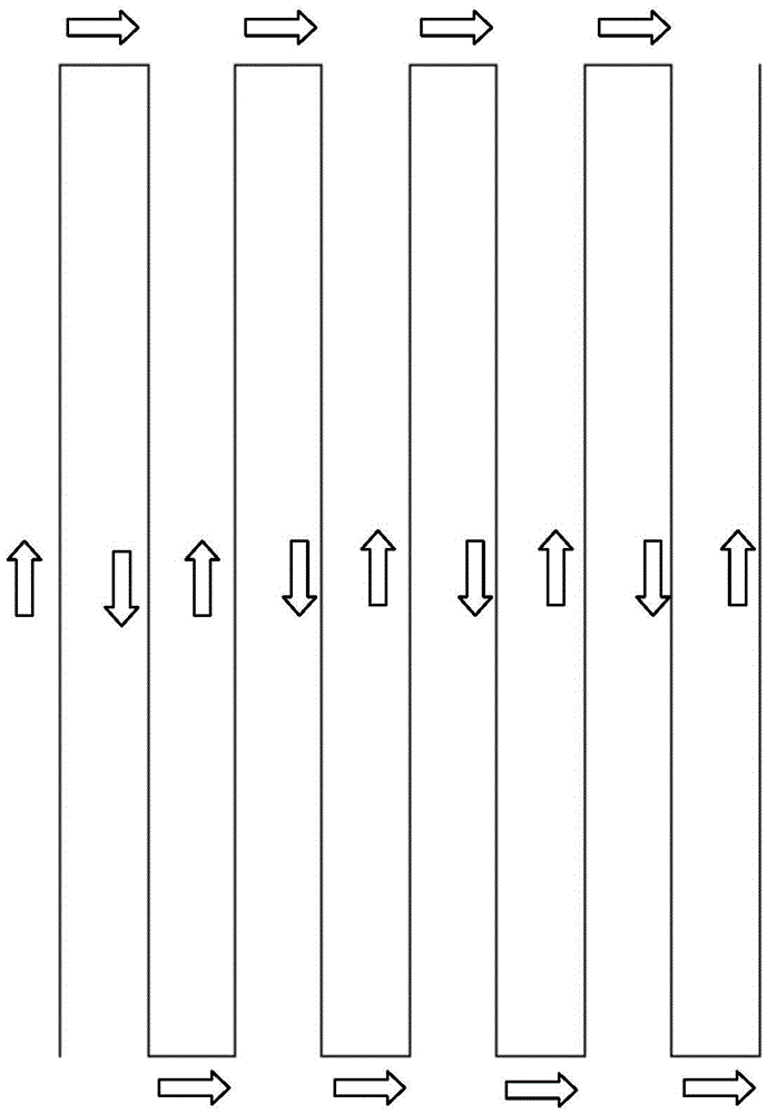
[0051] 2) According to the size, position and depth information of each component and chip inside the plastic packaged device obtained in step 1, determine the predetermined unsealing area (chip, component) of the plastic packaged device for unsealing positioning, and this area is slightly larger...

Embodiment 2

[0058] As an embodiment of the present invention, take TI company's TMS320 series BGA packaging DSP plastic packaging device (plastic packaging device with stronger corrosion resistance of molding material) as an example, the laser unsealing method includes the following steps:

[0059] 1) Before unsealing, the position and depth of each component and chip inside the plastic-encapsulated device are positioned by micro-focus X-rays to obtain the size, position and depth information of each component and chip inside the device. In general, unpacking only needs to expose the internal chips, inductors and resistors, so it is only necessary to remove the molding materials on the surface of these components and chips.

[0060] 2) According to the size, position and depth information of each component and chip inside the plastic packaged device obtained in step 1, determine the predetermined unsealing area (chip, component) of the plastic packaged device for unsealing positioning, and...

Embodiment 3

[0068] As an embodiment of the present invention, taking IR company's low-power field effect tube series and power module series plastic packaging device (copper bonding process device) as an example, the laser unsealing method includes the following steps:

[0069] 1) Before unsealing, the position and depth of each component and chip inside the plastic-encapsulated device are positioned by micro-focus X-rays to obtain the size, position and depth information of each component and chip inside the device. In general, unpacking only needs to expose the internal chips, inductors and resistors, so it is only necessary to remove the molding materials on the surface of these components and chips.

[0070] 2) According to the size, position and depth information of each component and chip inside the plastic packaged device obtained in step 1, determine the predetermined unsealing area (chip, component) of the plastic packaged device for unsealing positioning, and this area is slightl...


PUM

PropertyMeasurementUnit
poweraaaaaaaaaa
thicknessaaaaaaaaaa
thicknessaaaaaaaaaa

Abstract

The invention discloses a laser unsealing method. The method includes the steps that positions and depths of all elements and a chip in a plastic package device are positioned to obtain size, position and depth information of the elements and the chip in the device; according to the information, a preset unsealing area of the plastic package device is determined for unsealing and positioning; laser ablation is conducted on the plastic package device in a cross filling mode to remove molding materials on the surface of the plastic package device, so that inner lead bonding wires are just exposed out of a chip area, tin-lead welding points are just exposed near a resistor and a capacitor, and inductance is just exposed near an inductor. Acidic liquid is adopted to corrode a molding compound covering the chip till the chip is exposed. The method can well solve the problem that a traditional method can not unseal a plastic mixed integrated circuit easily, and effectively increases the unsealing success rate of the plastic package device.

Description

technical field [0001] The invention relates to the technical field of semiconductor unsealing, in particular to a laser unsealing method based on laser technology. Background technique [0002] Plastic-encapsulated device unsealing technology is mainly used in analysis fields such as destructive physical analysis (DPA) and failure analysis (FA) of electronic components. The purpose of the unsealing technology of plastic-encapsulated devices is to remove the original packaging of plastic-encapsulated devices through physical and chemical methods, and to expose the internal chip on the premise of retaining the original electrical characteristics, not damaging the chip, and not introducing secondary failures, and to conduct subsequent evaluations Analysis test. More and more new processes and technologies are gradually applied in the production and manufacture of plastic-encapsulated semiconductor devices, such as highly integrated multi-chip plastic-encapsulated devices, pla...

Claims


Application Information

Patent Timeline
Patent Type & Authority Applications(China)
IPC IPC(8): B23K26/362H01L21/306
CPCB23K26/361H01L21/30604
Inventor 贺峤王坦
Owner CASIC DEFENSE TECH RES & TEST CENT
Why Eureka
Try Eureka