Method for preparing low cost substrates

A technology of equipment and conductive parts, which is applied in the field of packaging of microelectronic devices and can solve problems such as chip assembly

Active Publication Date: 2016-05-25
INVENSAS CORP
View PDF12 Cites 5 Cited by
  • Summary
  • Abstract
  • Description
  • Claims
  • Application Information

AI Technical Summary

Problems solved by technology

Complex portable devices require...

Method used


Image

  • Method for preparing low cost substrates
  • Method for preparing low cost substrates
  • Method for preparing low cost substrates

Examples


Embodiment Construction

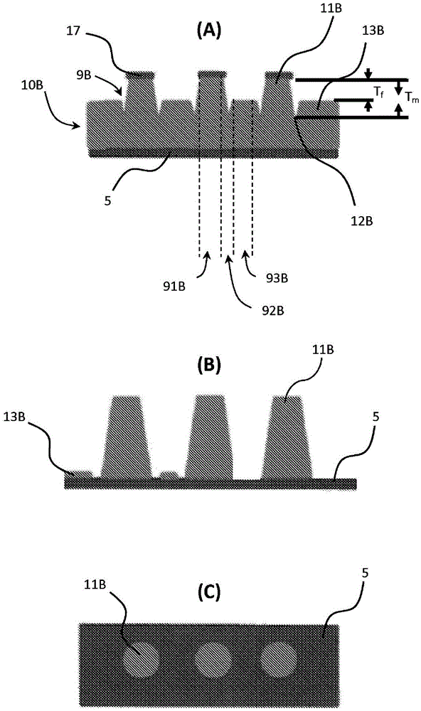
[0055] Components described herein, such as interposers, substrates, circuit panels, microelectronic elements, etc., may have one or both of insulating and dielectric structures at their outer surfaces in some arrangements. Thus, as used in this disclosure, a statement that a conductive element is "at" a surface of a component's dielectric structure means that when the component is not assembled with any other A theoretical point contact moving in the direction of the part surface from outside the part towards the part surface. Thus, a terminal or other conductive element at a surface of a component may protrude from such surface; may be flush with such surface; or may be recessed relative to such surface in the form of a hole or recess in the component.

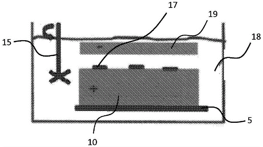
[0056] Now see attached picture, as figure 1 As shown, the conductive layer 10 can be attached to the support 5 together, or the conductive layer 10 can be attached to the support 5 . In one example, support 5 may comprise...


PUM


Abstract

A mask is formed over a first conductive portion of a conductive layer to expose a second conductive portion of the conductive layer. An electrolytic process is performed to remove conductive material from a first region and a second region of the second conductive portion. The second region is aligned with the mask relative to an electric field applied by the electrolytic process. The second region separates the first region of the second conductive portion from the first conductive portion. The electrolytic process is concentrated relative to the second region such that removal occurs at a relatively higher rate in the second region than in the first region.

Description

Background technique [0001] The present invention relates to the packaging of microelectronic devices, and more particularly to the packaging of semiconductor devices. [0002] Microelectronic devices typically include a thin sheet of semiconductor material, such as silicon or gallium arsenide, which is often referred to as a die or semiconductor chip. Semiconductor chips are typically provided as individual pre-packaged units. In some cell designs, the semiconductor chip is mounted to a substrate or chip carrier, which in turn is mounted to a circuit panel, such as a printed circuit board. [0003] Active circuitry is fabricated in a first side (eg front side) of the semiconductor chip. To facilitate electrical connection to active circuitry, the chip is provided with bond pads on the same side. The bond pads are typically arranged in a regular array, either around the edges of the die or, for many memory devices, in the center of the die. Bond pads are typically made of ...

Claims


Application Information

Patent Timeline
IPC IPC(8): C25F3/14H01L23/498H01L21/48
CPCC25F3/14H01L23/49827H01L21/486H01L2224/16225H01L2924/15311H01L23/49816H01L23/49822H05K3/07H05K2201/10378H01L21/6835H01L2221/68345H01L2221/68381C25F3/12H05K1/0212H05K1/115H01L21/4857H01L23/367H01L23/3733H01L23/49838H01L23/49866H01L24/17H01L25/0655H01L2924/01022H01L2924/01028H01L2924/01042H01L2924/01047H01L2924/0105H01L2924/01074H01L2924/01079H01L2924/15701H01L2924/15724H01L2924/15738H01L2924/15747H01L2924/15763
Inventor C·E·尤佐A·R·西塔拉姆
Owner INVENSAS CORP
Why Eureka
Try Eureka