Formation method of semiconductor structure

A semiconductor and strip-shaped technology, applied in the fields of semiconductor/solid-state device manufacturing, electrical components, circuits, etc., can solve problems such as poor contact between conductive plugs and interconnect lines, and reduced reliability of integrated circuits

Active Publication Date: 2016-06-08
SEMICON MFG INT (SHANGHAI) CORP
View PDF5 Cites 4 Cited by
  • Summary
  • Abstract
  • Description
  • Claims
  • Application Information

AI Technical Summary

Problems solved by technology

[0004] However, with the continuous advancement of semiconductor technology, the reduction of semiconductor process nodes and the improvement of integration have become a development trend. The feature size (CD, Critical Dimension) of semiconductor devices continues to shrink, and the dev...

Method used


Image

  • Formation method of semiconductor structure
  • Formation method of semiconductor structure
  • Formation method of semiconductor structure

Examples


Embodiment Construction

[0033] As mentioned in the background art, as the feature size of semiconductor devices shrinks and the device density increases, the reliability of the metal interconnection structure decreases.

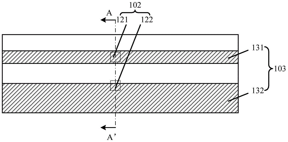
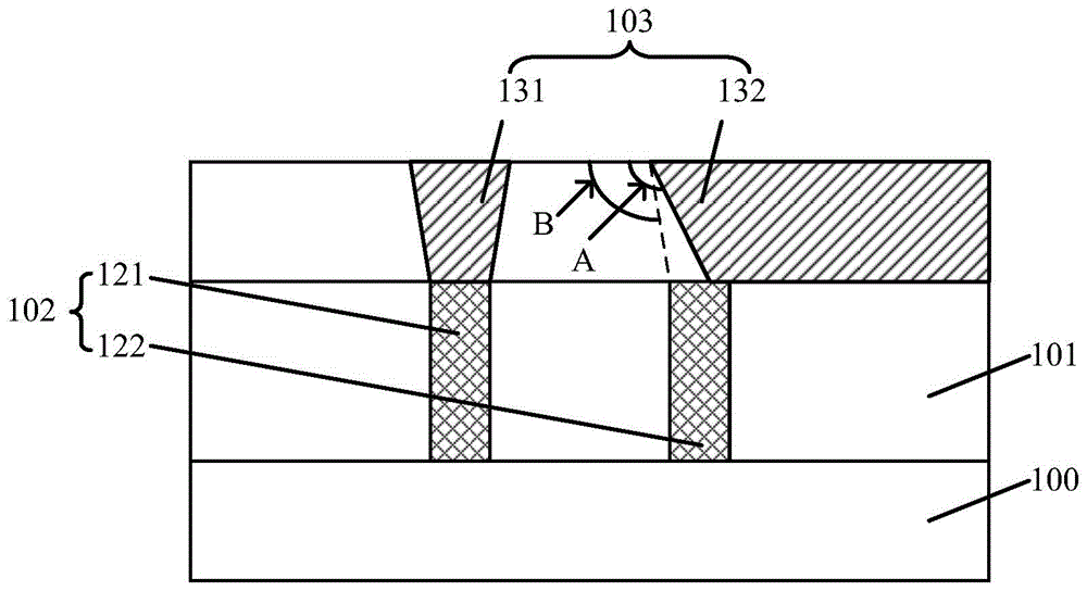
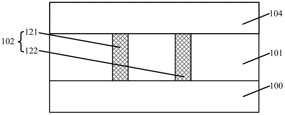
[0034] After research, please continue to refer to figure 1 and figure 2 , the conductive plug 102 includes a first plug 121 and a second plug 122; the interconnection line 103 includes a first interconnection line 131 located on the surface of the top 121 of the first plug, and a first interconnection line 131 located on the surface of the second plug 122 on the top surface of the second interconnect line 132 .

[0035] Wherein, the second interconnection line 132 is used to form a power supply circuit, therefore, the width of the second interconnection line 132 is greater than the width of the first interconnection line 131, so that the adjacent second interconnection line 132 and the first interconnection line The distance between one interconnection line 131 is relatively sma...


PUM


Abstract

The invention relates to a formation method of a semiconductor structure. The formation method comprises that a substrate is provided; a first dielectric layer is formed at the surface of the substrate, a sacrifice layer is formed in the first dielectric layer, and the surface of the sacrifice layer is leveled with the surface of the first dielectric layer; parts of the sacrifice layer and first dielectric layer are etched till the surface of the substrate is exposed, a first through hole is formed in the first dielectric layer; the residual sacrifice layer is removed, and an extension opening is formed in the first dielectric layer and communicates with the first through hole; a first conductive plug is formed in the first through hole and the extension opening; and a first conductive layer is formed at the surfaces of the first conductive plug and the first dielectric layer. The formed semiconductor structure is stable in electrical property and higher in reliability.

Description

technical field [0001] The invention relates to the technical field of semiconductor manufacturing, in particular to a method for forming a semiconductor structure. Background technique [0002] In the semiconductor manufacturing process, the back-end process (BEOL, Back-EndOfLine) is used to form a metal interconnection structure for realizing electrical interconnection between device structures after forming various device structures. The metal interconnection structure includes a conductive plug and an electrical interconnection line on top of the conductive plug. Among them, the conductive plug is often used for electrical interconnection between the upper and lower conductive layers, and the electrical interconnection line is used to form a circuit structure together with the semiconductor device. [0003] figure 1 and figure 2 is a structural schematic diagram of a metal interconnection structure, figure 2 Yes figure 1 The schematic diagram of the top view struc...

Claims


Application Information

Patent Timeline
IPC IPC(8): H01L21/768
CPCH01L21/76897H01L21/76816
Inventor 何其暘黄敬勇
Owner SEMICON MFG INT (SHANGHAI) CORP
Why Eureka
Try Eureka