

Organic solar cell with exciton blocking and sunlight sensitivity enhancing integrated type hole transport layer and preparation method of organic solar cell
A hole transport layer and solar cell technology, applied in the field of green solar energy, can solve the problems of mismatch of injection and transmission rates, many unclear mechanisms, low short-circuit current, etc., so as to reduce the dark current component and electron leakage current, The effect of balancing transport properties and preventing exciton quenching
- Summary
- Abstract
- Description
- Claims
- Application Information
AI Technical Summary
Problems solved by technology
Method used
Image

Examples
Embodiment 1
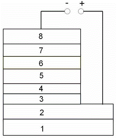
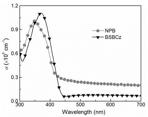
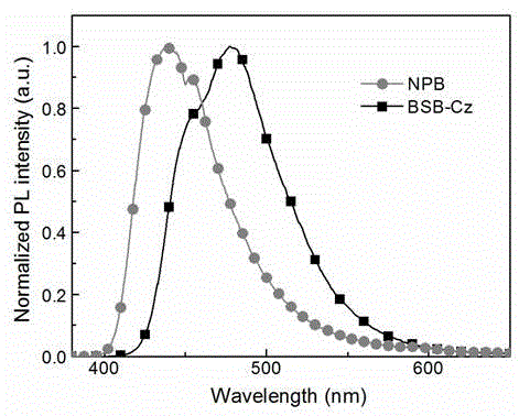
[0043] In this example, see figure 1 , an organic solar cell with an integrated hole transport layer for exciton blocking and sunlight sensitization, which consists of a substrate layer 1, a transparent conductive anode layer 2, a hole injection layer 3, and an exciton blocking layer from bottom to top 4. The donor layer 5, the acceptor layer 6, the electron transport layer 7 and the electrode cathode layer 8 are composed of a total of 8 functional layers. The donor layer 5 is made of organic solar cell materials with narrow band and strong absorption. The acceptor layer 6 is made of fullerene, and the material of the exciton blocking layer 4 is a wide bandgap hole transport material with ultraviolet absorption and almost no absorption of visible light, and the energy level of the exciton blocking layer 4 is the same as that of the donor layer 5 match.
[0044] In this embodiment, the ITO substrate composed of the substrate layer 1 and the transparent conductive anode layer 2...
Embodiment 2
[0048] This embodiment is basically the same as Embodiment 1, especially in that:
[0049] In this example, see figure 1 , select a transparent ITO glass substrate etched into a certain template as the anode, and the thickness of the ITO glass substrate is 150 nm. Use lotion, acetone, deionized water, and isopropanol to clean ultrasonically for 20 minutes, blow dry with nitrogen, and UV / O 3 Process for 15 minutes and set aside. The hole injection layer MoO was deposited on the ITO glass substrate by vacuum evaporation 3 , the thickness is 10nm, then deposit the exciton blocking layer BSB-Cz, the thickness is controlled at 8-20nm, then deposit the donor SubPc, the thickness is 7-20nm and the acceptor layer C 60 , with a thickness of 30-50nm, and then deposit Bphen, an electron transport layer material, with a thickness of 5-10nm, and then replace the mask plate to vapor-deposit the cathode metal, and the vapor-deposited metal Al is the cathode, with a thickness of 100nm.
...
PUM
| Property | Measurement | Unit |
|---|---|---|
| Thickness | aaaaa | aaaaa |
| Thickness | aaaaa | aaaaa |
| Thickness | aaaaa | aaaaa |
Abstract
Description
Claims
Application Information