

Deviation signal producing circuit and multiport configurable PUF circuit
A technology of deviation signal and circuit generation, applied in the direction of adjusting electrical variables, control/regulating systems, instruments, etc., can solve the problem of current input current size deviation and other problems, and achieve the effect of improving uniqueness
- Summary
- Abstract
- Description
- Claims
- Application Information
AI Technical Summary
Problems solved by technology
Method used
Image

Examples
Embodiment 1
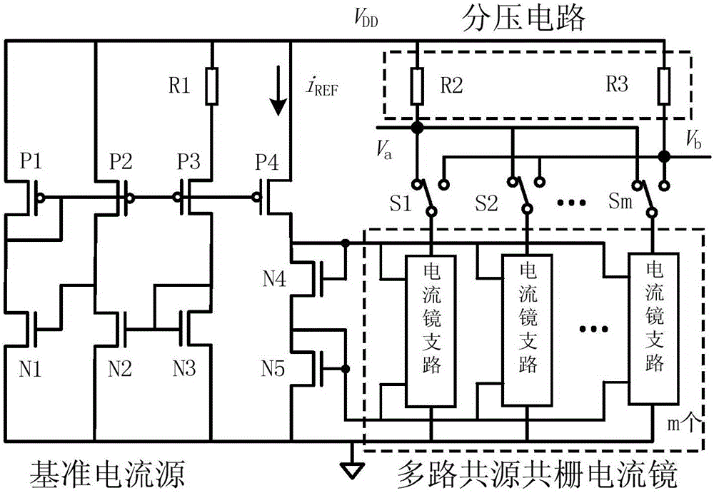
[0026] Embodiment one: if figure 1 As shown in Figure 2(a), a deviation signal generating circuit includes a reference current source, a voltage divider circuit, a multi-channel cascode current mirror and m logic control signal switches S1, S2, ..., Sm, where m is An integer greater than or equal to 2;
[0027] The reference current source includes a first PMOS transistor P1, a second PMOS transistor P2, a third PMOS transistor P3, a fourth PMOS transistor P4, a first NMOS transistor N1, a second NMOS transistor N2, a third NMOS transistor N3, and a fourth NMOS transistor N4, the fifth NMOS transistor N5 and the first resistor R1, the voltage divider circuit includes the second resistor R2 and the third resistor R3; the source of the first PMOS transistor P1, the source of the second PMOS transistor P2, the fourth PMOS transistor P4 The source of the first resistor R1, one end of the second resistor R2 and one end of the third resistor R3 are all connected to the power supply...
Embodiment 2
[0028] Embodiment two: if figure 1 As shown in Figure 2(a), a deviation signal generating circuit includes a reference current source, a voltage divider circuit, a multi-channel cascode current mirror and m logic control signal switches S1, S2, ..., Sm, where m is An integer greater than or equal to 2;
[0029]The reference current source includes a first PMOS transistor P1, a second PMOS transistor P2, a third PMOS transistor P3, a fourth PMOS transistor P4, a first NMOS transistor N1, a second NMOS transistor N2, a third NMOS transistor N3, and a fourth NMOS transistor N4, the fifth NMOS transistor N5 and the first resistor R1, the voltage divider circuit includes the second resistor R2 and the third resistor R3; the source of the first PMOS transistor P1, the source of the second PMOS transistor P2, the fourth PMOS transistor P4 The source of the first resistor R1, one end of the second resistor R2 and one end of the third resistor R3 are all connected to the power supply,...
PUM
 Abstract
Description
Claims
Application Information