Preparation method of vertical ultraviolet LED chip

A LED chip and ultraviolet technology, which is applied in the field of vertical ultraviolet LED chip preparation, can solve the problems of high price and unstable preparation process, and achieve the effects of low production cost, facilitating current flow, and overcoming absorption

Inactive Publication Date: 2016-06-15
HEBEI UNIV OF TECH +1
View PDF7 Cites 8 Cited by
  • Summary
  • Abstract
  • Description
  • Claims
  • Application Information

AI Technical Summary

Problems solved by technology

CN201110212605.3 discloses a TCO-type conductive DBR vertical blue LED chip and its manufacturing method. Its main technical solution is to use conductive DBR as a reflector and TCO as a current spreading layer. TCO has a strong absorption capacity for deep ultraviolet rays. Not suitable for UV vertical LED chips, and the TCO and conductive DBR are expensive and the manufacturing process is unstable

Method used


Image

  • Preparation method of vertical ultraviolet LED chip
  • Preparation method of vertical ultraviolet LED chip
  • Preparation method of vertical ultraviolet LED chip

Examples


Embodiment 1

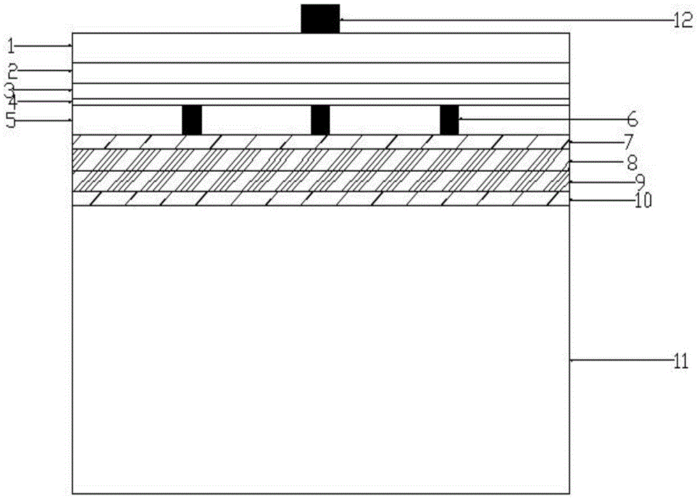
[0044] The preparation method of a vertical ultraviolet LED chip of the present embodiment, the steps are as follows:

[0045] The first step is to grow the N-type epitaxial layer, the multiple quantum well layer and the P-type epitaxial layer sequentially on the sapphire substrate wafer by MOCVD, and use the mass percentage concentration of 98% H on the grown epitaxial wafer. 2 SO 4 with a mass percentage concentration of 30% H 2 O 2 The mixed solution with volume ratio=3:1 was heated to 80°C, soaked for 10 minutes, then rinsed with deionized water for 5 minutes, and finally dried with a spin dryer for 20 minutes;

[0046] In the second step, on the surface of the P-type epitaxial layer of the sapphire substrate treated in the first step, an ultra-thin metal Ni / Ag was evaporated with an electron beam evaporation stage as a current spreading layer, and the thickness of Ni was controlled exist The thickness of Ag is controlled at The metal current spreading layer is requ...

Embodiment 2

[0053] The preparation method of a vertical ultraviolet LED chip of the present embodiment, the steps are as follows:

[0054] The first step is the same as in Example 1;

[0055] In the second step, on the surface of the P-type epitaxial layer of the sapphire substrate treated in the first step, an ultra-thin metal Ni / Ag was evaporated with an electron beam evaporation stage as a current spreading layer, and the thickness of Ni was controlled exist The thickness of Ag is controlled at The metal current spreading layer is required to form an ohmic contact with the P-type epitaxial layer after the next step of annealing;

[0056] In the third step, except that the annealing temperature is 370°C and the annealing time is 8 minutes, the rest is the same as in Example 1;

[0057] The fourth step is to prepare a DBR layer on the Ni / Ag metal current spreading layer annealed in the third step, and the material used is SiO 2 and TiO 2 Evaporation source, use electron beam evapo...

Embodiment 3

[0062] The preparation method of a vertical ultraviolet LED chip of the present embodiment, the steps are as follows:

[0063] The first step is the same as in Example 1;

[0064] In the second step, on the surface of the P-type epitaxial layer of the sapphire substrate treated in the first step, an ultra-thin metal Ni / Ag was evaporated with an electron beam evaporation stage as a current spreading layer, and the thickness of Ni was controlled exist The thickness of Ag is controlled at The metal current spreading layer is required to form an ohmic contact with the P-type epitaxial layer after the next step of annealing;

[0065] In the third step, except that the annealing temperature is 400°C and the annealing time is 10 minutes, the rest is the same as in Example 1;

[0066] The fourth step is to prepare a DBR layer on the Ni / Ag metal current spreading layer annealed in the third step, and the material used is SiO 2 and TiO 2 Evaporation source, use electron beam evap...


PUM

PropertyMeasurementUnit
thicknessaaaaaaaaaa

Abstract

The invention discloses a preparation method of a vertical ultraviolet LED chip, in particular, a method applicable for manufacturing a semiconductor device which is provided with at least one potential jump barrier and is suitable for light emission. A metal current spreading layer Ni/Ag and a DBR are adopted to replace a metal reflective layer of the vertical ultraviolet LED chip, the thickness of Ni in the metal current spreading layer Ni/Ag being controlled in the range of 5 to 10 Angstroms, and the thickness of Ag in the metal current spreading layer Ni/Ag being controlled in the range of 10 to 40 Angstroms. According to the DBR, at first, a SiO2 layer of which the thickness ranges from 4200 to 4400 Angstroms is formed through electron beam evaporation; and TiO2 and SiO2 are evaporated alternately, and evaporation is performed for 4 to 20 cycles, and the thickness of the TiO2 in each evaporation cycle ranges from 278 to 348 Angstroms, and the thickness of the SiO2 in each evaporation cycle ranges from 477 to 596 Angstroms. With the preparation method of the invention adopted, problems caused by the absorption of light by a metal reflective layer in the prior art can be improved, and the illumination brightness of the vertical ultraviolet LED chip can be improved.

Description

technical field [0001] The technical scheme of the present invention relates to a method suitable for manufacturing a semiconductor device with at least one potential hopping barrier, which is specially suitable for light emission, specifically a method for preparing a vertical ultraviolet LED chip. Background technique [0002] With the rapid development of LED technology, the application range of UV LEDs with wavelengths ranging from 350 to 280 nm is becoming wider and wider. Compared with traditional UV light sources, UV LEDs are more energy efficient, have longer lifespans, and do not contain toxic substances. However, compared with InGaN-based near-ultraviolet LEDs or blue-light LEDs, the quantum efficiency of ultraviolet LEDs is very low. In addition, the absorption of ultraviolet light by metal mirrors directly leads to the output power of ultraviolet LEDs being only 5% of the input power. -8%. [0003] The existing flip-chip and vertical UV LED chips are mainly mad...

Claims


Application Information

Patent Timeline
Patent Type & Authority Applications(China)
IPC IPC(8): H01L33/00H01L33/10H01L33/14H01L33/40
CPCH01L33/0054H01L33/10H01L33/14H01L33/405
Inventor 张保国周朝旭甄珍珍李晓波
Owner HEBEI UNIV OF TECH
Why Eureka
Try Eureka