Check patentability & draft patents in minutes with Patsnap Eureka AI!

Etching method

A technology of dry etching and wet etching, which is applied in the direction of electrical components, semiconductor/solid-state device manufacturing, circuits, etc., and can solve problems such as deep trenches that cannot be etched

Pending Publication Date: 2016-06-22
BEIJING NAURA MICROELECTRONICS EQUIP CO LTD
View PDF5 Cites 6 Cited by
  • Summary
  • Abstract
  • Description
  • Claims
  • Application Information

AI Technical Summary

Problems solved by technology

[0007] It can be seen from Table 1 that when the above etching method is used to etch the SiC substrate, the etching rate can only reach 140nm / min, which can only meet the requirements of etching shallow trenches (grooves with a depth less than 10 μm) on the SiC substrate. ) and cannot meet the requirements for etching deep trenches (grooves with a depth greater than 10 μm) on SiC substrates

Method used


Image

  • Etching method
  • Etching method
  • Etching method

Examples


Embodiment Construction

[0042] Specific embodiments of the present invention will be described in detail below in conjunction with the accompanying drawings. It should be understood that the specific embodiments described here are only used to illustrate and explain the present invention, and are not intended to limit the present invention.

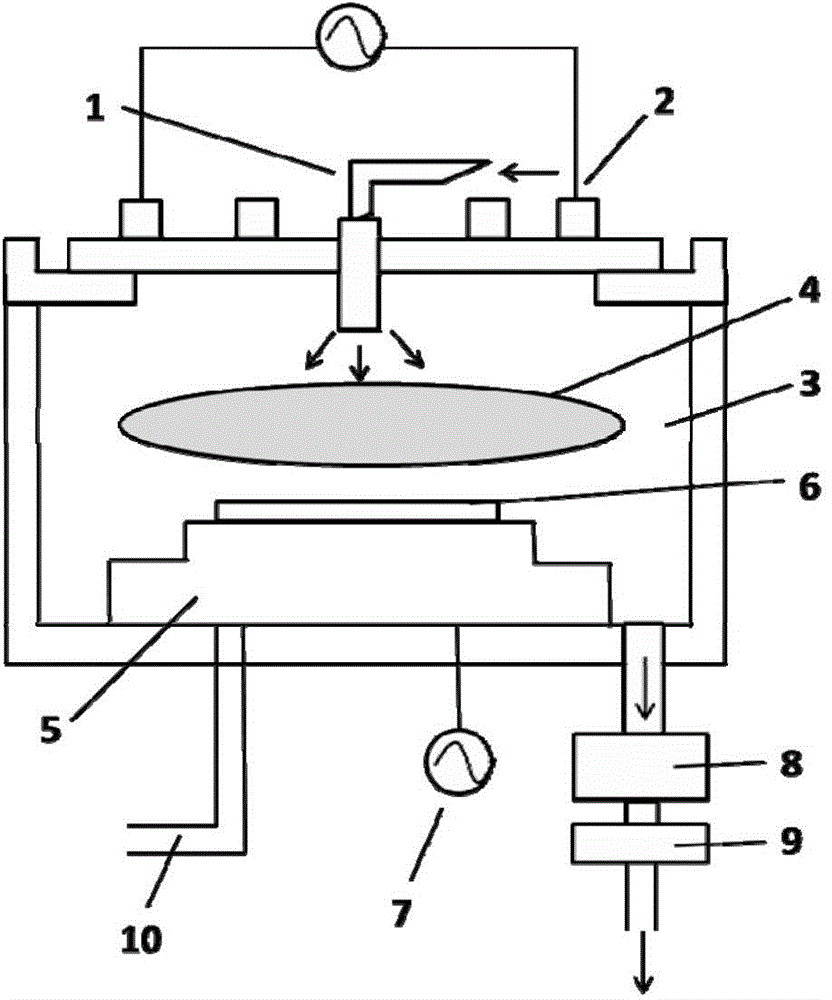
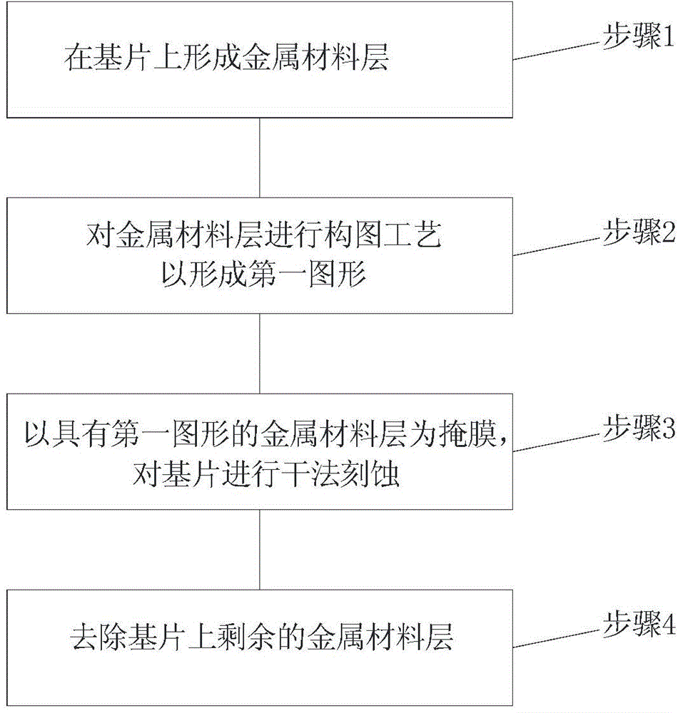
[0043] Such as figure 1 As shown, the present invention provides an etching method, wherein the etching method includes:

[0044] Step 1: forming a metal material layer on the substrate;

[0045] Step 2: performing a patterning process on the metal mask layer to form a first pattern;

[0046] Step 3: using the metal material layer having the first pattern as a mask, performing dry etching on the substrate;

[0047] Step 4: removing the remaining metal material layer on the substrate.

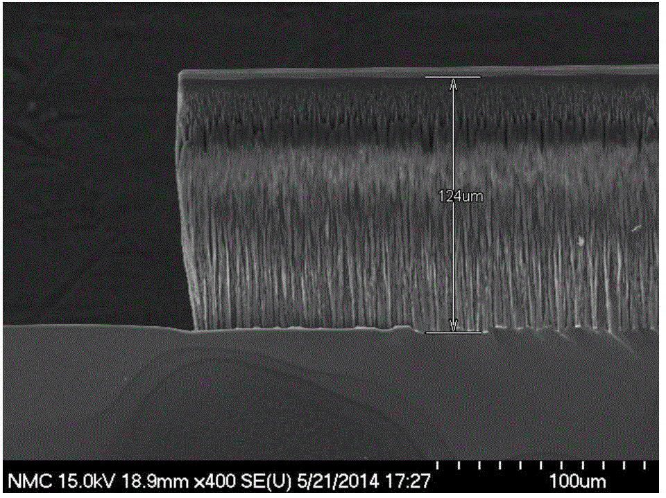
[0048] In the etching method provided by the present invention, the metal material is used to make the mask required for etching the substrate. Compared with the conventional ...


PUM


Abstract

The invention provides an etching method, which includes: step 1: forming a metal material layer on a substrate; step 2: performing a patterning process on the metal material layer to form a first pattern; step 3: forming a first pattern with The metal material layer in the first pattern is used as a mask, and dry etching is performed on the substrate; step 4: removing the remaining metal material layer on the substrate. In the etching method provided by the present invention, the metal material is used to make the mask required for etching the substrate. Compared with the conventional photoresist mask layer, the metal mask layer has a larger hardness. , therefore, there is a larger etching selectivity ratio between the first pattern and the substrate, so that the metal material layer having the first pattern is not easily etched by the etching gas. Therefore, the present invention The provided etching method is more suitable for etching deep grooves on the substrate.

Description

technical field [0001] The invention relates to the field of semiconductor processing, in particular to an etching method. Background technique [0002] Silicon carbide (SiC) materials have the advantages of large band gap, high breakdown field strength, and small dielectric constant. It is known as the third-generation semiconductor material with very broad prospects. Etching technology is a key supporting technology in the development of silicon carbide devices. In the process of manufacturing silicon carbide devices, fast and high-selectivity etching technology is essential. The etching precision, etching damage, and residues on the etching surface of the etching process all have a fatal impact on the development and performance of silicon carbide devices. However, due to the high hardness and stable chemical properties of silicon carbide materials, wet etching cannot meet the requirements. At present, most of the commonly used silicon carbide etching methods are dry et...

Claims


Application Information

Patent Timeline
IPC IPC(8): H01L21/04H01L21/3065
Inventor 周娜苏子铎袁仁志谢秋实
Owner BEIJING NAURA MICROELECTRONICS EQUIP CO LTD
Features
  • R&D
  • Intellectual Property
  • Life Sciences
  • Materials
  • Tech Scout
  • Unparalleled Data Quality
  • Higher Quality Content
  • 60% Fewer Hallucinations
Learn More