Low-capacitance and low-voltage semiconductor overvoltage protection device

An over-voltage protection device and low-voltage technology, which is applied in semiconductor devices, semiconductor/solid-state device manufacturing, electrical components, etc., can solve the problems of high production cost, complicated production process, complex structure, etc., and achieve simple structure and simple realization process , the effect of area reduction

Inactive Publication Date: 2016-06-29
KUNSHAN HAIXIN ELECTRONICS CO LTD
View PDF7 Cites 5 Cited by
  • Summary
  • Abstract
  • Description
  • Claims
  • Application Information

AI Technical Summary

Problems solved by technology

Although it can also meet the requirement of junction capacitance below 30pF, the structure is still relatively complicated, the manufacturing process is complicated, and the manufacturing cost is relatively high.

Method used


Image

  • Low-capacitance and low-voltage semiconductor overvoltage protection device
  • Low-capacitance and low-voltage semiconductor overvoltage protection device
  • Low-capacitance and low-voltage semiconductor overvoltage protection device

Examples


Embodiment

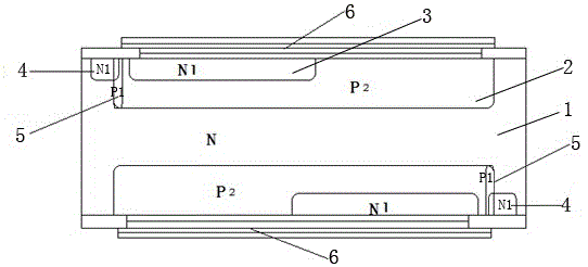
[0035] Such as figure 2 As shown, a low-capacitance low-voltage semiconductor overvoltage protection device, the chip layer includes an N-type substrate 1, a P2 base region 2 and an N-type region 3 are diffused symmetrically above and below the N-type substrate 1, and an emitter N-type The doped region 4 has a P1 base region 5 diffused between the emitter N-type doped region 4 and the P2 base region 2, the P1 base region 5 is a high-concentration P-type doped base region, and the P2 base region 2 is a low-concentration P-type doped region. Heterogene region. The surface of the chip layer is a metalized electrode region 6 . The metallized electrode region 6 includes four layers, aluminum 1 μm, titanium 0.3 μm, nickel 0.7 μm, silver 0.5 μm.

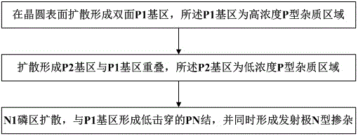
[0036] Such as image 3 Shown, a kind of preparation method of low-capacitance low-voltage semiconductor overvoltage protection device of the present invention comprises the following steps:

[0037] S01: Diffusion on the surface of th...


PUM


Abstract

The invention discloses a low-capacity and low-voltage semiconductor overvoltage protection device. The chip layer includes an N-type substrate, and a P2 base region, an N-type region and an emitter N-type doped region are diffused symmetrically above and below the N-type substrate. A P1 base region is diffused in the emitter N-type doped region and the P2 base region, and the P1 and P2 are P-type variable doped base regions. The base area diffusion is divided into two parts to achieve variable doping base area, the P1 base area is a high-concentration P-type doping diffusion, and the P2 base area is a low-concentration P-type doping diffusion, so that the area of ​​high-concentration regions on both sides of the PN junction It is greatly reduced to ensure the low-voltage and over-voltage protection functions, and at the same time, the parasitic junction capacitance of the PN junction is greatly reduced, and the design goal of low capacitance is realized. The process is simple and the cost is low.

Description

technical field [0001] The invention relates to a low-capacity overvoltage protection device, in particular to a low-capacity and low-voltage semiconductor overvoltage protection device. Background technique [0002] With the rapid development of communication / communication technology, the development of high-definition video and high-speed network is becoming more and more rapid, and the signal interface of related equipment has higher and higher requirements for the capacitance of low-voltage overvoltage protection devices. [0003] The vertical design structure of the current mainstream solid discharge tube, such as figure 1 As shown, it generally includes two processes of double-sided boron diffusion and double-sided phosphorus diffusion. The junction capacitance is parasitic at the junction of the P base region and the N-type substrate and the edge low-level pass-through region. Since low-voltage products require diffusion at both ends of the PN junction to reach a hi...

Claims


Application Information

Patent Timeline
Patent Type & Authority Applications(China)
IPC IPC(8): H01L29/87H01L29/10H01L21/329
CPCH01L29/87H01L29/1012H01L29/66121
Inventor 赵海
Owner KUNSHAN HAIXIN ELECTRONICS CO LTD
Why Eureka
Try Eureka