White-light LED chip manufacturing method
A technology of LED chips and manufacturing methods, which is applied to electrical components, circuits, semiconductor devices, etc., can solve the problems of high cost, complicated operation, and low work efficiency, and achieve the effects of low cost, simple operation method, and high work efficiency
- Summary
- Abstract
- Description
- Claims
- Application Information
AI Technical Summary
Problems solved by technology
Method used
Image
Examples
Embodiment 1
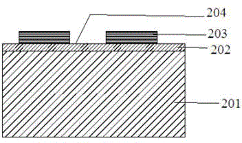
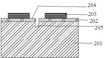
[0016] As shown in FIG. 2, a method for manufacturing a white LED chip includes preparing a GaN LED wafer with a vertical structure on a silicon substrate 201, such as Figure 2a 202 in the figure is the bonding metal layer, and the gallium nitride LED 203 is separated by the cutting line 204; the 355nm ultraviolet laser emitted by the laser is focused to the middle position of the cutting line 204 on the upper surface of the silicon substrate 201, forming a depth of 30±5μm , a groove 205 with a width of 20±2 μm, such as Figure 2b ; Use titanium dioxide doped silica gel to configure white glue 206 with high reflectivity to fill in the cutting line 204 and groove 205, grind and thin the white glue so that its height is flush with the upper surface of the LED chip, as Figure 2c , wherein the mass percentage of titanium dioxide in the white glue is 50%, and then cured at a baking temperature of 150°C for 1h; a layer of phosphor powder 207 is coated on the gallium nitride LED 20...
Embodiment 2
[0018] Another method for manufacturing a white LED chip includes preparing a GaN LED wafer with a vertical structure on a silicon substrate 301, such as Figure 3a , 302 in the figure is the bonding metal layer, the gallium nitride LED 303 is separated by the cutting line 304; the white glue 305 with high reflectivity is configured with zinc oxide doped silica gel and filled in the cutting line 304, and the white glue is ground and thinned, so that Its height is flush with the upper surface of the LED chip, such as Figure 3b , wherein the mass percentage of zinc oxide in the white glue is 60%, and then the curing time is 1h at a baking temperature of 150°C; a layer of fluorescent adhesive film 306 is pasted on the gallium nitride LED303 and baked and cured, such as Figure 3c As shown; the wafer is cut along the dicing road 304 to obtain a single white LED chip surrounded by white glue, such as Figure 3d shown.
PUM
 Abstract
Description
Claims
Application Information


