De-gassing chamber

A technology of air chamber and chamber, which is applied in the field of degassing chamber, can solve the problems that restrict the production efficiency of PVD equipment, and achieve the effects of shortening the process preparation time, simplifying the heating process, and improving production capacity

Active Publication Date: 2016-07-06
BEIJING NAURA MICROELECTRONICS EQUIP CO LTD
View PDF3 Cites 2 Cited by
  • Summary
  • Abstract
  • Description
  • Claims
  • Application Information

AI Technical Summary

Problems solved by technology

[0008] The cycle of processing each wafer in the above-mentioned existing degassing chamber is close to 80 seconds, and the preparation of the copper barrier layer and the copper seed layer takes about 40 to 45 seconds, which is 1 / 2 of the time of the degassing process. Therefore, the current The long working cycle of the degassing chamber directly restricts the production efficiency of PVD equipment

Method used


Image

  • De-gassing chamber
  • De-gassing chamber
  • De-gassing chamber

Examples


Embodiment Construction

[0020] The present invention will be described below in conjunction with examples.

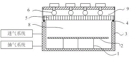
[0021] The degassing chamber of the present invention includes a vacuum chamber and a radiation source. The wafer to be processed is placed in the vacuum chamber, and the radiation source is arranged in the vacuum chamber to directly radiate and heat the wafer to be processed below it.

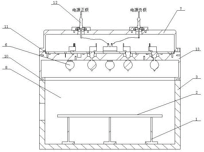
[0022] image 3 It is a preferred embodiment of the present invention. As shown in the figure, the cavity of the vacuum chamber 8 is composed of a lower cavity 3, a radiation source mounting base 13, and an upper cover 7. The joint surface of the cavity 3 and the mounting base 13 is sealed by a sealing ring 10, and the upper cover 7 The joint surface with the mounting base 13 is sealed by an O-ring 11, the radiation source 6 is installed on the mounting base 13, the upper cover 7 is provided with a terminal 12 with a sealing structure, and the radiation source 6 is connected to the vacuum chamber through the ...


PUM


Abstract

The invention discloses a de-gassing chamber. The de-gassing chamber comprises a vacuum chamber and a radiation source, wherein the radiation source is arranged in the vacuum chamber for directly carrying out radiant heating on a to-be-processed chip placed in the vacuum chamber below. According to the de-gassing chamber, the conventional method of arranging the radiation source outside the vacuum chamber is changed, and the radiation source is directly arranged in the vacuum chamber, so that the defect caused by the conventional quartz window is eliminated, and therefore, the heating flow is simplified, the process preparation time of a de-gassing process is shortened, the period of the de-gassing process is greatly shortened, and conditions are created for increasing the yield of PVD equipment.

Description

technical field [0001] The invention relates to a degassing chamber used in the process of preparing thin films by physical vapor deposition technology. Background technique [0002] Physical vapor deposition or sputtering (Sputtering) deposition technology is the most widely used type of thin film manufacturing technology in the semiconductor industry. It generally refers to the thin film preparation process that uses physical methods to prepare thin films; Controlled sputtering (MagnetronSputtering) technology is mainly used for the deposition of metal films such as aluminum and copper to form metal contacts and metal interconnections. [0003] In the physical vapor deposition process (300mm and above wafers), four process steps are required to complete the entire physical vapor deposition process. The four process steps are in order: 1) Degas (Degas); 2) Precleaning (PreClean) ; 3) Preparation of copper barrier layer (Ta / Tan); 4) Preparation of copper seed layer (Cu). f...

Claims


Application Information

Patent Timeline
Patent Type & Authority Applications(China)
IPC IPC(8): C23C14/56
CPCC23C14/564
Inventor 佘清侯珏叶华
Owner BEIJING NAURA MICROELECTRONICS EQUIP CO LTD
Why Eureka
Try Eureka