
Vertical transition connector for chip package, substrate structure and fabrication method

A vertical transition and chip packaging technology, which is applied in semiconductor/solid-state device manufacturing, electric solid-state devices, semiconductor devices, etc., can solve the problems of high design and processing costs, low assembly efficiency, and high price, and achieve high assembly efficiency and low cost. Low, small size effect

Active Publication Date: 2016-07-06
THE 13TH RES INST OF CHINA ELECTRONICS TECH GRP CORP
View PDF6 Cites 3 Cited by
  • Summary
  • Abstract
  • Description
  • Claims
  • Application Information

AI Technical Summary

Problems solved by technology

For slightly larger module and component-level products, especially products in the RF / microwave field, the existing vertical interconnection technology is still lacking, or the size is large, the assembly efficiency is low (such as coaxial cables, insulators), or the price Expensive, pressure fastened (like snap buttons), or expensive to design and process (like flexible printed boards)

Method used


Image

  • Vertical transition connector for chip package, substrate structure and fabrication method
  • Vertical transition connector for chip package, substrate structure and fabrication method
  • Vertical transition connector for chip package, substrate structure and fabrication method

Examples


Embodiment Construction

[0022] The present invention will be further described in detail below in conjunction with the accompanying drawings and specific embodiments.

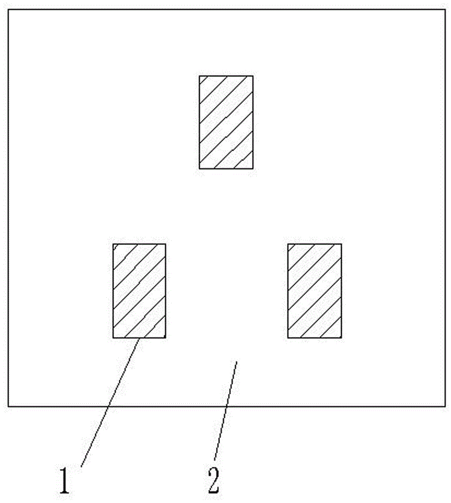
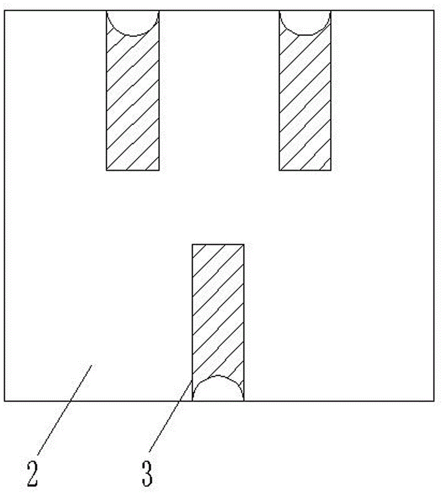
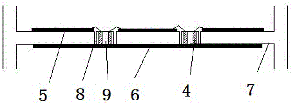
[0023] For the structure of vertical transition connectors for chip packaging, see figure 1 , figure 2 As shown, it includes an insulating connection base 2, at least one conductor hole is provided in the vertical direction in the insulation connection base 2, a solid conductor post 4 is fixed in the conductor hole, and an upper pad 1 is provided on the upper surface of the solid conductor post 4, and the solid conductor The lower surface of the pillar 4 is provided with a lower pad 3 .

[0024] Wherein, the upper pad 1 is a bondable coating, and the coating meets the bonding process requirements; the lower pad 3 is a solderable coating, and the coating meets the surface mount reflow soldering process requirements.

[0025] To further illustrate, the shape structure of the connecting base 2 is a column; the column is preferably a c...


PUM


Abstract

The invention discloses a vertical transition connector for chip package, a substrate structure and a fabrication method, and relates to the technical field of chip package. The vertical transition connector comprises an insulation connection substrate, wherein at least one conductor hole is formed in the insulation connection substrate in a vertical direction, a solid conductor post is fixedly arranged in the conductor hole, an upper bonding pad is arranged on the upper surface of the solid conductor post, and a lower bonding pad is arranged on the lower surface of the solid conductor post. The vertical transition connector has the characteristics of small size, low cost and high interconnection density, the assembly efficiency can be improved, the transmission signal frequency can be increased, and the fabrication method is simple and convenient and is suitable for automatic and miniature production application at a large scale.

Description

technical field [0001] The invention relates to the technical field of chip packaging, in particular to a vertical transition connector for chip packaging, a substrate structure and a manufacturing method. Background technique [0002] At present, in order to adapt to the development of miniaturization and multi-function, electronic equipment and devices are developing towards three-dimensional structure. For the realization of the three-dimensional structure, there are many and mature technologies at the chip packaging level, such as chip stacking, chip flip chip, chip bonding (TSV process), etc. For slightly larger module and component-level products, especially products in the RF / microwave field, the existing vertical interconnection technology is still lacking, or the size is large, the assembly efficiency is low (such as coaxial cables, insulators), or the price Expensive, require pressure fixing (such as fur buttons), or high design and processing costs (such as flexi...

Claims


Application Information

Patent Timeline
IPC IPC(8): H01L23/538H01L21/768
CPCH01L23/5384H01L21/76895
Inventor 常青松郝金中徐达王合利王志会
Owner THE 13TH RES INST OF CHINA ELECTRONICS TECH GRP CORP
Learn More