High-voltage electronic static discharge (ESD) protection device with positive-negative (PN) junction auxiliary trigger silicon controlled rectifier-laterally diffused metal oxide semiconductor (SCR-LDMOS) structure

A SCR-LDMOS, ESD protection technology, applied in the field of electronics, can solve problems such as latch-up, achieve the effect of avoiding the latch-up effect, improving ESD protection capability, and improving ESD robustness

Active Publication Date: 2016-07-06
ANHUI LONGXINWEI TECH CO LTD
View PDF5 Cites 11 Cited by
  • Summary
  • Abstract
  • Description
  • Claims
  • Application Information

AI Technical Summary

Problems solved by technology

Low hold voltage V h It can reduce the power consumption when the ESD current is turned on and discharged, but it is used as the ESD protection of the power supply pin, except for the trigger voltage V t1 higher than the power supply VDD, the maintenance voltage V h also needs to be higher than V DD
If the maintenance voltage V h below the chip V DD , it is very prone to latch-up phenomenon

Method used


Image

  • High-voltage electronic static discharge (ESD) protection device with positive-negative (PN) junction auxiliary trigger silicon controlled rectifier-laterally diffused metal oxide semiconductor (SCR-LDMOS) structure
  • High-voltage electronic static discharge (ESD) protection device with positive-negative (PN) junction auxiliary trigger silicon controlled rectifier-laterally diffused metal oxide semiconductor (SCR-LDMOS) structure

Examples


Embodiment Construction

[0016] Below in conjunction with accompanying drawing, technical scheme of the present invention is described in further detail:

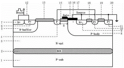
[0017] as attached figure 2 Shown is a high-voltage ESD protection device with a PN junction-assisted trigger SCR-LDMOS structure, including a P-type silicon substrate 1, a buried oxide layer 2 is provided on the P-type silicon substrate, and a drift region 3 is provided on the buried oxide layer. An N-buffer region 5, a P region 4, and a P-body region 8 are sequentially provided above the drift region from left to right; the N-buffer region 5 is sequentially provided with a first drain heavily doped N+ region 7 and the first drain heavily doped P+ region 6; the P-body region 8 is provided with a second source heavily doped N+ region 9 and a second source heavily doped P+ region 10 in sequence from left to right and the third source heavily doped P+ region 11; a first thin oxide layer 13 is provided between the first drain heavily doped P+ region...


PUM


Abstract

The invention discloses a high-voltage electronic static discharge (ESD) protection device with a positive-negative (PN) junction auxiliary trigger silicon controlled rectifier-laterally diffused metal oxide semiconductor (SCR-LDMOS) structure. The high-voltage ESD protection device comprises a P-type substrate, wherein a buried oxygen layer is arranged on the P-type substrate, a shift region is arranged on the buried oxygen layer, an N-buffer region, a P region and a P-body region are sequentially arranged on the shift region from left to right, a first drain heavily-doping N+ region and a first drain heavily-doping P+ region are sequentially arranged in the N-buffer region from left to right, a second source heavily-doping N+ region, a second source heavily-doping P+ region and a third source heavily-doping P+ region are sequentially arranged in the P-body region from left to right, and the P region and the second source heavily-doping P+ region are connected through a wire. When a drain of the ESD protection device encounters a positive ESD pulse, a reverse bias PN junction is used for helping improving the hole carrier concentration before trigger starting, and a trigger voltage V<t1> is reduced; and moreover, with the introduction of the reverse bias PN junction into the device, the positive and negative feedback effect of a parasitic SCR can be effectively prevented, thus, the maintaining voltage V<h> of the device can be effectively increased, and the latch-up effect of the device is prevented.

Description

technical field [0001] The invention relates to the field of electronic technology, in particular to a high-voltage ESD protection device with a PN junction auxiliary trigger SCR-LDMOS structure. Background technique [0002] Silicon-controlled rectifier (SiliconControlledRectifier, SCR) has received extensive attention in ESD protection because of its strong robustness. However, the LDMOS structure with embedded SCR structure (SCR-LDMOS) has some fatal problems: [0003] 1. The turn-on trigger voltage V of the SCR-LDMOS device t1 too high. SCR relies on low-doped N-well and P-well avalanche breakdown, triggering voltage V t1 Relatively higher than the breakdown voltage of the gate oxide layer of the device inside the pin, it does not meet the ESD protection requirements of the device. [0004] 2. Due to the NPN and PNP positive feedback, the SCR-LDMOS device maintains the voltage V h Very low, usually only around 5V. Low hold voltage V h It can reduce the power consu...

Claims


Application Information

Patent Timeline
Patent Type & Authority Applications(China)
IPC IPC(8): H01L27/02
CPCH01L27/0251H01L27/0255H01L27/0296
Inventor 滕国兵成建兵陈旭东郭厚东
Owner ANHUI LONGXINWEI TECH CO LTD
Why Eureka
Try Eureka