Laser processing device with linear array optical lens assembly with micro cylindrical lenses in cylindrical distribution

A micro-cylindrical lens and optical lens technology, which is applied in optics, optical components, laser welding equipment, etc., can solve the problems of difficult processing, not very strict optical path precision, and large processing area, and achieve the effect of improving processing efficiency

Inactive Publication Date: 2016-07-13
CHANGCHUN UNIV OF SCI & TECH
View PDF6 Cites 22 Cited by
  • Summary
  • Abstract
  • Description
  • Claims
  • Application Information

AI Technical Summary

Problems solved by technology

Although the laser interference micro-nano processing method has the advantages of low cost, high precision, and large processing area, in order to obtain micro-nano structures of different sizes, various process parameters need to be precisely adjusted. In this regard, the processing is relatively difficult. In addition, This method requires high precision of the optical path
[0005] However, in some fields, there is an urgent need for a laser micro-nano processing method that not only has low processing cost, high precision, and high efficiency, but also can easily change the processing size and shape. At the same time, the optical path of the laser processing device used is adjusted Easy, not very strict requirements on optical path accuracy

Method used


Image

  • Laser processing device with linear array optical lens assembly with micro cylindrical lenses in cylindrical distribution
  • Laser processing device with linear array optical lens assembly with micro cylindrical lenses in cylindrical distribution
  • Laser processing device with linear array optical lens assembly with micro cylindrical lenses in cylindrical distribution

Examples


Embodiment Construction

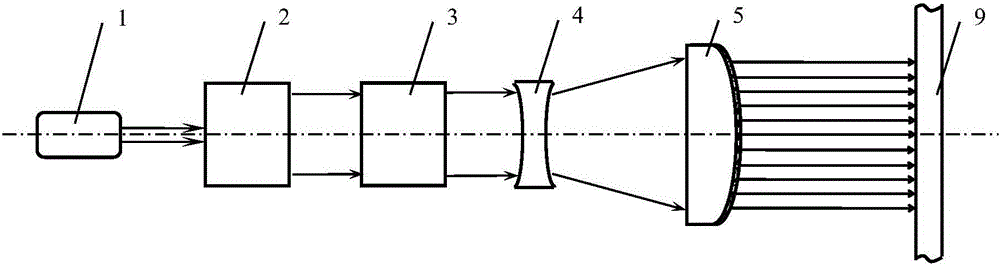
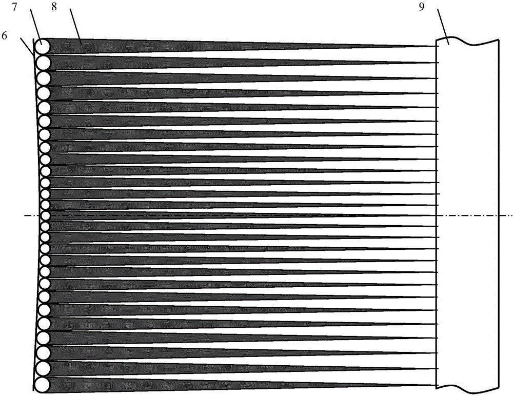
[0016] Such as figure 1 As shown, a laser light source 1, a collimating beam expander 2, a beam shaping mirror 3, a double-concave lens 4, and a linear array of micro-cylindrical lenses with cylindrical distribution are optically arranged coaxially in sequence.

[0017] The laser light source 1 is a high-power Nd:YAG pulsed solid-state laser with a wavelength of 1064nm, a pulse width of 8ns, a single pulse energy of 2J, a beam exit diameter of Φ8mm, and a divergence angle of 3mrad.

[0018] The beam expansion factor of the collimating beam expander 2 is 6.25, and it is composed of multiple optical lenses, the lens material is K9 glass, the mirror surfaces of the multiple optical lenses are all coated with AR1064nm, the incident diameter of the beam is Φ10mm, and the outgoing diameter of the beam is Φ50mm .

[0019] The beam shaping mirror 3 shapes the laser beam with circular spot and Gaussian distribution of light energy into a laser beam with square spot and uniform distrib...


PUM

PropertyMeasurementUnit
wavelengthaaaaaaaaaa

Abstract

The invention relates to a laser processing device with a linear array optical lens assembly with micro cylindrical lenses in cylindrical distribution, and belongs to the technical field of laser processing. A conventional laser direct writing micro-nano processing method is low in processing efficiency. The laser processing device disclosed by the invention is characterized in that a laser source, a collimating beam expanding mirror, a beam shaping mirror, a biconcave lens, and the linear array optical lens assembly with micro cylindrical lenses in cylindrical distribution are sequentially, optically and coaxially arrayed; the beam shaping mirror is used for shaping laser beams with round light spots and light energy in gaussian distribution into laser beams with square light spots and light energy in uniform distribution; the linear array optical lens assembly with micro cylindrical lenses in cylindrical distribution adopts the structure that a plurality of micro cylindrical lenses are arrayed on a convex cylindrical mirror surface of a plano-convex cylindrical mirror and parallel to a cylindrical generatrix, besides, the diameters of the micro cylindrical lenses are gradually increased from the micro cylindrical lens positioned at the highest point of the convex cylindrical mirror surface to the micro cylindrical lens positioned at the lowest point of the convex cylindrical mirror surface, and symmetrical surfaces of a bar-shaped wedge-shape laser beam emitted from each micro cylindrical lens are mutually parallel; the plane mirror of the plano-convex cylindrical mirror faces towards the biconcave lens.

Description

technical field [0001] The invention relates to a laser processing device with a linear array optical lens of micro-cylindrical lenses distributed on a cylindrical surface, which can process micro-nano structures on the surface of a workpiece, and belongs to the technical field of laser processing. Background technique [0002] Laser micro-nano machining is a laser processing technology that processes micro-nano structures on the surface of workpieces. The existing laser micro-nano processing methods related to the invention include laser direct writing and laser interference. [0003] The laser direct writing micro-nano processing method refers to the use of an adjustable laser beam to directly expose the surface of the workpiece to form the desired micro-nano structure. The laser direct writing micro-nano processing method has the advantages of high processing precision, complex morphology and structure, and a wide range of processed materials. However, due to the point-b...

Claims


Application Information

Patent Timeline
Patent Type & Authority Applications(China)
IPC IPC(8): B23K26/064B23K26/364B23K26/70G02B27/09
CPCB23K26/364B23K26/0648B23K26/702G02B27/0961G02B27/0966
Inventor 李永亮高龙岳周玮琦
Owner CHANGCHUN UNIV OF SCI & TECH
Why Eureka
Try Eureka