Etching method for directly forming multi-layer graphene film in graphene prepared through CVD method

A multi-layer graphene and graphene layer technology, applied in graphene, chemical instruments and methods, inorganic chemistry, etc., can solve the problem of limiting the large-scale application of graphene films, destroying the integrity of graphene layers, and mixing impurities in graphene layers and other problems, to achieve the effect of reducing the production process and production cost, less impurities, and less structure damage

Active Publication Date: 2016-07-13
WUXI GRAPHENE FILM +1
View PDF4 Cites 11 Cited by
  • Summary
  • Abstract
  • Description
  • Claims
  • Application Information

AI Technical Summary

Problems solved by technology

However, these processes are complicated, and it is very easy to destroy the integrity of the graphene layer during the process, and it is easy to mix impurities on the surface of the graphene layer, which affects the performance of the superimposed graphene. Not only the process yield is low, but also the cost is high. Limiting the large-scale application of graphene films

Method used


Image

  • Etching method for directly forming multi-layer graphene film in graphene prepared through CVD method

Examples


Embodiment 1

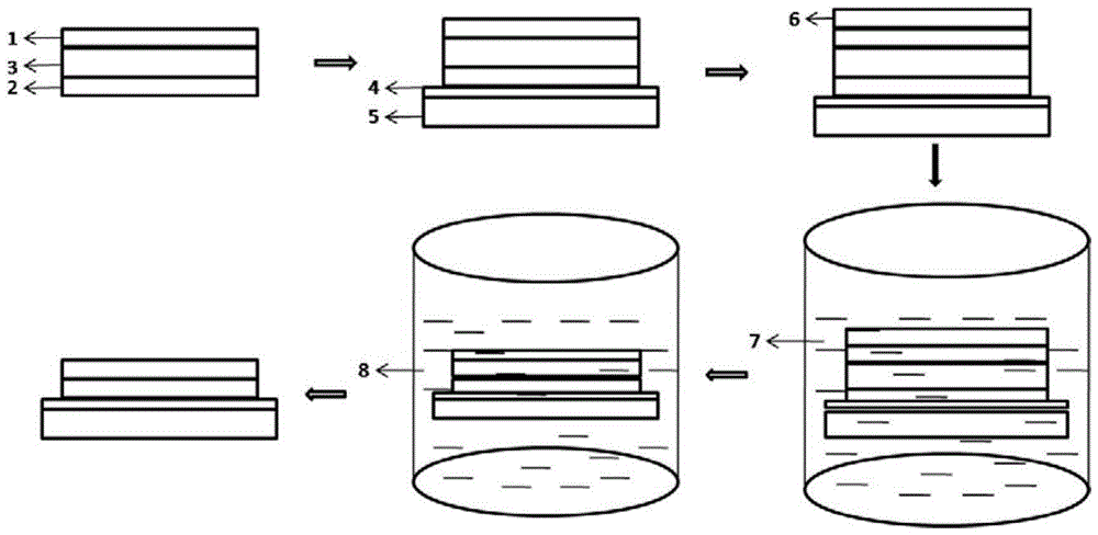
[0040] The etching method for directly forming a double-layer graphene film in graphene prepared by CVD method, the process flow can be found in figure 1 , wherein, 1: upper graphene layer; 2: bottom graphene; 3: copper foil, 4: adhesive layer, 5: substrate, 6: PMMA; 7: etching solution, 8: PMMA cleaning agent.

[0041] The specific operation steps are as follows:

[0042] 1. The graphene film (single layer) is grown on the copper foil surface by CVD method, wherein the thickness of the copper foil is 1-1000 μm, preferably 5-30 μm;

[0043] 2. Apply an adhesive layer on the surface of the substrate, and then attach the side of the copper foil containing graphene to the substrate containing the adhesive layer (another method is to first coat the adhesive layer on the copper foil side, and then attach it to the substrate ), the viscous layer material can be one or a combination of heat curing glue, ultraviolet (UV) curing glue, thermoplastic glue, etc., and then under UV or hea...

Embodiment 2

[0052] CVD method prepares the etching method that directly forms four-layer graphene thin film in graphene, basically with embodiment 1, difference is in the following points:

[0053] 1) Using nickel foil as a growth substrate to grow two layers of graphene;

[0054] 2) A mixed solution of hydrochloric acid and hydrogen peroxide is used as an etching solution, the concentration of hydrochloric acid is 0.05-5 mol / L, and the concentration of hydrogen peroxide is 0.05-5 mol / L.

Embodiment 3

[0056] CVD method prepares the etching method that directly forms six-layer graphene film in graphene, basically with embodiment 1, difference is in the following points:

[0057] 1) Three layers of graphene are grown on both sides of the copper foil;

[0058] 2) A ferric perchloride solution with a concentration of 0.05-5 mol / L is used as the etching solution.


PUM

PropertyMeasurementUnit
thicknessaaaaaaaaaa
thicknessaaaaaaaaaa
thicknessaaaaaaaaaa

Abstract

The invention discloses an etching method for directly forming a multi-layer graphene film in graphene prepared through a CVD method. The etching method comprises the following steps: 1) bonding any side of a growth substrate where grapheme is grown through the CVD method with a substrate; 2) coating a protective glue solution at the other side of the growth substrate treated in the step 1), and then, roasting the growth substrate; 3) putting the growth substrate treated in the step 2) into an etching solution to etch, and removing the growth substrate clamped between graphene layers at the two sides, enabling the graphene layers, which are originally positioned at the two sides of the growth substrate separately, to automatically and tightly fit to form a double-layer graphene film, and getting out the double-layer graphene film; 4) cleaning the double-layer graphene film formed in the step 3 with water, roasting the double-layer graphene film, removing surface protective glue, cleaning the double-layer graphene film, and drying the double-layer graphene film, thereby obtaining the multi-layer graphene film.

Description

technical field [0001] The invention relates to an etching method for growing graphene by a chemical vapor deposition (CVD) method, and belongs to the field of etching in the electronic industry. Background technique [0002] Graphene is a single-atom-layer two-dimensional crystal in which carbon atoms are tightly packed in a hexagonal structure. In addition to its excellent optical, thermal, and mechanical properties, graphene’s carriers behave like photons, and their intrinsic mobility can be controlled. Up to 2×105cm 2 / (V·S)(J.Appl.Phys.2011,109,093702.), this excellent electrical property makes it have great application value in high-frequency electronic devices. [0003] The chemical vapor deposition CVD method is considered to be the most promising method for preparing high-quality and large-area graphene, and it is the most potential method for the industrial production of graphene films. The specific process of the chemical vapor deposition CVD method is: the hydr...

Claims


Application Information

Patent Timeline
Patent Type & Authority Applications(China)
IPC IPC(8): C01B31/04
CPCC01B2204/04
Inventor 秦喜超谭化兵王炜
Owner WUXI GRAPHENE FILM
Why Eureka
Try Eureka