

Fingerprint identification system based on raster structure and microprism array
A technology of fingerprint identification and grating structure, which is applied in the direction of prism, diffraction grating, character and pattern recognition, etc. It can solve the problems of difficult miniaturization, difficult miniaturization, and large overall structure, so as to increase the contrast of fingerprint images and reduce finger scattering The effect of precise optical path control
- Summary
- Abstract
- Description
- Claims
- Application Information
AI Technical Summary
Problems solved by technology
Method used
Image

Examples
Embodiment 1
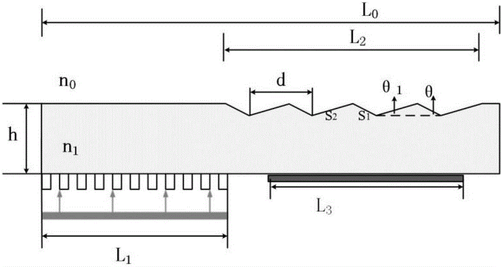
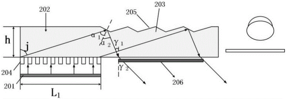
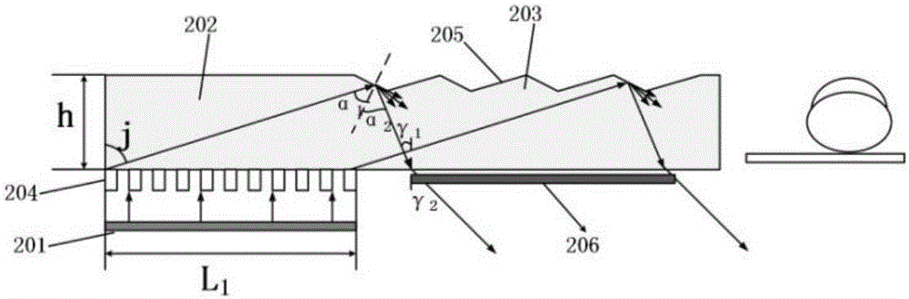
[0060] From formula (5), we can see that, In order to get a smaller thickness h, in L 1 Under certain circumstances, the closer the diffraction angle j should be set to 90°, the better. Combining with formula (2), considering the lateral propagation, the diffraction angle j should be set to 85°θ 1 is 5°, the corresponding grating period is 370nm, and the incident light wavelength is 550nm. For the case of air normal incidence, the air refractive index n 0 =1, the waveguide material is the most commonly used polymethyl methacrylate, its refractive index n 1 = 1.49, the refractive index of the finger surface is about 1.39-1.42, combined with formula (13), it can be obtained that 16.11° Figure 5 As shown, the illuminance of valley lines in the fingerprint pattern received by the imaging device is close to 0, and the contrast is close to 95%. As the angle increases, the fingerprint pattern appears slightly blurred, and the contrast ratio drops to 89%. This is because the small...
Embodiment 2
[0062] For the case of air normal incidence, the air refractive index n 0 =1, waveguide refractive index n 1 =1.49, the refractive index of the finger surface is about 1.39~1.42, set θ=25°, the diffraction angle j is 85°, θ 1 If it is set to 5°, when the unit width d of the microprism is different, the obtained fingerprint patterns are also different. Using software simulation to simulate the width of the triangle base of different microprism sections, the results are as follows Figure 6 shown. It is ideal for the case of d=0.05mm. When d is larger than 0.1mm, due to the increase of the width of the bottom edge, the depth of the prism section will increase under the condition of a certain angle θ, which makes it more difficult for fingers to touch, so the fingerprint pattern Streaks will appear. Therefore, for the selection of the unit width d of the microprism, the smaller the better, but considering the limitation of the processing technology, d=0.05mm is more suitable. ...
Embodiment 3
[0064] For the case of air normal incidence, the air refractive index n 0 =1, waveguide refractive index n 1 =1.49, the refractive index of the finger surface is about 1.39, set θ=25°, the diffraction angle j is 85°, d is 0.05mm, when θ 1 When the settings are different, the obtained fingerprint patterns are also slightly different, such as Figure 7 As shown, if θ 1 When the smaller is 1°, then θ 1 The side of the prism where it is located will reflect part of the light, thus reducing the useful light and reducing the contrast of the image; if θ 1 When the maximum is 35°, the fingerprint detection area is more rugged, and the finger is not easy to touch the bottom of the microprism, thus reducing the image contrast and user experience; when θ 1 When it is 5°, the ruggedness is appropriate, and a high-contrast and clear fingerprint pattern is obtained.
[0065] Experiments show that the present invention utilizes the diffraction of the grating, the light of the light sour...
PUM
 Abstract
Description
Claims
Application Information