Wiring board with embedded interposer integrated with stiffener and method of making the same
A manufacturing method and reinforcement layer technology, applied in printed circuit manufacturing, circuit, printed circuit, etc., can solve problems such as poor reliability of chip-level connections
- Summary
- Abstract
- Description
- Claims
- Application Information
AI Technical Summary
Problems solved by technology
Method used
Image
Examples
Embodiment 1
[0099] Figure 1-24 It is a diagram of a manufacturing method of a circuit board in the first embodiment of the present invention, which includes an interposer 11 , a positioning member 14 , a resin molded reinforcing layer 30 and a build-up circuit 40 .
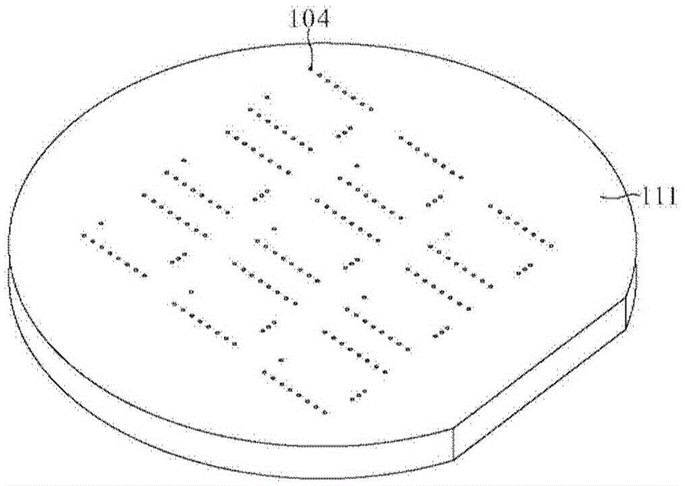
[0100] figure 1 and 2 They are respectively a cross-sectional view and a bottom perspective view of the substrate 111 , which includes a first surface 101 , an opposite second surface 102 , and a blind hole 104 formed on the first surface 101 . The substrate 111 may be made of silicon, glass or ceramics, and has a thickness of 50 μm to 500 μm. The blind holes 104 have a depth of 25 microns to 250 microns. In this embodiment, the substrate 111 is a silicon wafer and has a thickness of 200 micrometers, and the blind hole 104 has a depth of 150 micrometers.
[0101] image 3 It is a cross-sectional view after forming the metallized via 116 . Metallized vias 116 are formed in the substrate 111 by depositing metal in the bl...
Embodiment 2
[0128] Figure 28-37 It is a diagram of a circuit board manufacturing method according to the second embodiment of the present invention, wherein the manufacturing method does not use a carrier film.
[0129] For the purpose of brief description, any descriptions in the above-mentioned embodiment 1 that can be used for the same application are incorporated here, and it is not necessary to repeat the same descriptions.
[0130] Figure 28 It is a sectional view of multiple sets of positioning elements 14 on the sacrificial carrier 13 . In this embodiment, after the positioning member 14 is formed on the sacrificial carrier 13, the sacrificial carrier 13 is then processed into a configuration having a plurality of protrusions 131 and a flange 133. This configuration can usually be It is formed by etching or mechanical carving (carving). Here, these bump parts 131 protrude from the flange part 133, and may have a protruding height of 0.1 to 1.0 mm, and the flange part 133 is l...
Embodiment 3
[0144] Figure 39-46 It is a diagram of the circuit board manufacturing method according to the third embodiment of the present invention, which includes the step of attaching the finished interposer to the sacrificial carrier.
[0145] For the purpose of brief description, any descriptions in the above embodiments that can be used for the same application are incorporated here, and the same descriptions do not need to be repeated.
[0146] Figure 39 and 40 They are respectively a cross-sectional view and a top perspective view of a positioning member 14 on the sacrificial carrier 13 . In this embodiment, the sacrificial carrier 13 is processed to have a configuration of a protruding portion 131 and a flange portion 133 , and then the positioning member 14 is formed on the protruding portion 131 of the sacrificial carrier 13 . Here, the protrusion portion 131 protrudes from the flange portion 133 , and the flange portion 133 extends laterally from the protrusion portion 13...
PUM
 Abstract
Description
Claims
Application Information


