Active region contact windows of dynamic random access memory and manufacturing method of active region contact windows

A dynamic random access and manufacturing method technology, which is applied in semiconductor/solid-state device manufacturing, semiconductor/solid-state device components, and electrical solid-state devices, etc. The effect of short-circuiting the line and the contact window or lowering the threshold voltage, reducing the resistance value, and avoiding the step height difference

Active Publication Date: 2016-07-20
WINBOND ELECTRONICS CORP
View PDF3 Cites 5 Cited by
  • Summary
  • Abstract
  • Description
  • Claims
  • Application Information

AI Technical Summary

Problems solved by technology

The shrinking chip size not only poses great challenges to exposure machine technology and etching capabilities, but also causes

Method used


Image

  • Active region contact windows of dynamic random access memory and manufacturing method of active region contact windows
  • Active region contact windows of dynamic random access memory and manufacturing method of active region contact windows
  • Active region contact windows of dynamic random access memory and manufacturing method of active region contact windows

Examples


Example Embodiment

[0053] Please refer to the accompanying drawings in this article in order to fully appreciate the concept of the present invention. The accompanying drawings show embodiments of the present invention. However, the present invention can also be practiced in many different forms and should not be construed as being limited to the embodiments described below. In fact, the embodiments are only provided to make the present invention more detailed and complete, and to fully convey the scope of the present invention to those skilled in the art.

[0054] In the drawings, the size and relative size of each layer and area may be exaggerated for clarity.

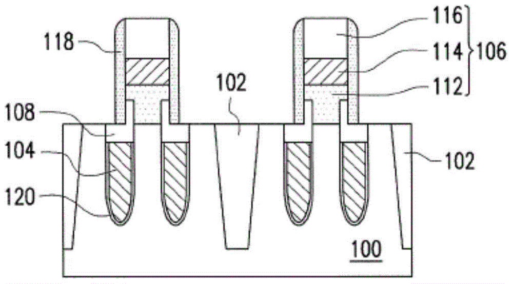
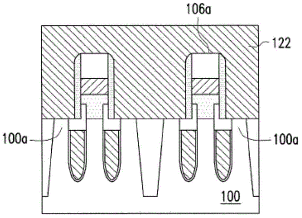
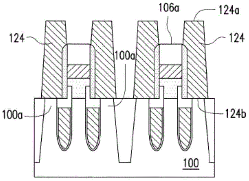
[0055] Figure 1A to Figure 1D It is a schematic cross-sectional view of the manufacturing process of the active area contact window of a dynamic random access memory according to the first embodiment of the present invention.

[0056] Please refer to Figure 1A , The dynamic random access memory of this embodiment at least includes a substra...


PUM


Abstract

The invention provides active region contact windows of a dynamic random access memory and a manufacturing method of the active region contact windows. The manufacturing method of active regions of the memory comprises the step as follows a conducting layer is formed on on a substrate to cover contact window regions and bit lines. The dynamic random access memory at least comprises the substrate, an isolating structure in the substrate, the active regions, embedded-type word lines and the bit lines, wherein the active regions are partitioned through the isolating structure; the embedded-type word lines pass through the active regions; the bit lines are arranged on the substrate; and each active region comprises a plurality of contact window regions. After the conducting layer is formed, the conducting layer out of the contact window regions is removed to form a plurality of active region contact windows; and an insulating layer is formed on the substrate to cover the active region contact windows.

Description

technical field [0001] The invention relates to a dynamic random access memory (DRAM), in particular to an active area contact window (AAcontact) of the dynamic random access memory and a manufacturing method thereof. Background technique [0002] With the impact of the expansion of large manufacturers, the memory market environment is becoming increasingly severe. Each major manufacturer is actively working on the research and development of process technology and reducing the cost of the process. The main way to reduce the cost is to reduce the cost of the process. The shrinking chip size not only poses great challenges to exposure machine technology and etching capabilities, but also causes various adverse effects due to the continuous shrinking of the word line pitch and the isolation structure of the memory array. For example, the resistance value Rs of the contact window, due to the shrinking of the chip size, the volume of the contact window decreases, which in turn g...

Claims


Application Information

Patent Timeline
IPC IPC(8): H01L23/528H01L21/768H01L27/115H01L21/8247
Inventor 陈佩瑜欧阳自明
Owner WINBOND ELECTRONICS CORP
Why Eureka
Try Eureka