CMOS image sensor technology-based NP type single-photon avalanche diode

A single-photon avalanche and image sensor technology, applied in semiconductor devices, electrical components, circuits, etc., can solve problems such as limitations and poor noise characteristics, and achieve the effects of enhancing response, improving noise characteristics, and reducing dark counts

Inactive Publication Date: 2016-07-27
XIANGTAN UNIV
View PDF4 Cites 25 Cited by
  • Summary
  • Abstract
  • Description
  • Claims
  • Application Information

AI Technical Summary

Problems solved by technology

Traditional CMOS single photon avalanche diodes are implemented using P+/Nwell junctions, and the

Method used


Image

  • CMOS image sensor technology-based NP type single-photon avalanche diode
  • CMOS image sensor technology-based NP type single-photon avalanche diode
  • CMOS image sensor technology-based NP type single-photon avalanche diode

Examples


Embodiment Construction

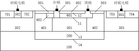
[0019] figure 1 It is an NP-type single-photon avalanche diode (SPAD) based on CMOS image sensor technology provided by the present invention, and its basic structure includes: a deep N well (200) is arranged above a P-type silicon substrate (100); a P well (301 ) is formed above and in contact with the deep N well (200); lightly doped guard rings (401, 402) are provided around the P well (301); N+ regions (601, 602) are formed in Above the P well (301) and overlaps with the lightly doped guard rings (401, 402) to a certain extent; N+ regions (601, 602) and lightly doped guard rings (401, 402) are provided with heavy doping Doped P-type regions (801, 802, 803), covering the entire surface of (601, 602) and (401, 402) except for the cathode and anode contacts; lightly doped guard rings around (401, 402) There are P wells (302, 303), and the P well region (302, 303) leads to the substrate electrode through the P+ region (502, 503); the heavily doped P type region (801, 802, 803...


PUM


Abstract

The inventioN discloses a CMOS image sensor technology-based NP type single-photon avalanche diode (SPAD). The basic structure of the SPAD comprises a deep N-well arranged above a P-type silicon substrate; a P-well formed above the deep N-well; a lightly-doped guard ring surrounding the P-well; a N+ region formed above the P-well and overlapped with the guard ring; a PN-junction formed between the N+ region and the P-well; a cathode electrode and an anode electrode respectively led out of the N+ and P+; a heavily-doped P-type region formed above the N+ region and the guard ring; a P-well surrounding the guard ring and a substrate electrode led out of the P+. According to the technical scheme of the invention, through forming the heavily-doped P-type region on the surface of the N+ region, the dark counting caused by defects on the interface of an NP-type SPAD device can be reduced. Based on the effective layout technique, the dark counting caused by defects in the STI is reduced. Based on the effective guard ring technique, the edge breakdown of the SPAD device is prevented. Through applying an appropriate bias voltage between the electrodes, the response within the blue band is enhanced.

Description

technical field [0001] The invention relates to a structure of an NP-type single-photon avalanche diode based on a CMOS image sensor technology. Background technique [0002] Single-photon detection is a detection method of extremely weak light, which is widely used in astronomy, biochemistry and medical diagnosis and other fields. Because the energy of a single photon is extremely low, it is difficult to directly extract this weak signal with common detection methods. In order to observe the changes caused by the absorption of a single photon in matter, an associated amplification mechanism must exist. Using the principle of the photoelectric effect, single-photon detectors based on photomultiplier tubes (PMTs) and avalanche photodiodes can be employed. [0003] Early single-photon detection used the method of photomultiplier tubes. As a single photon detector, PMT has the advantages of high gain, large photosensitive area and low dark count, but it needs to work at high...

Claims


Application Information

Patent Timeline
IPC IPC(8): H01L31/107H01L31/0352
Inventor 金湘亮杨红姣
Owner XIANGTAN UNIV
Why Eureka
Try Eureka