Memory reading method and digital memory device

A technology for memory and data reading, which is applied in static memory, read-only memory, information storage, etc., and can solve problems such as difficult to support serial or non-gate flash memory high-speed code mapping applications

Active Publication Date: 2016-08-03
WINBOND ELECTRONICS CORP
View PDF8 Cites 3 Cited by
  • Summary
  • Abstract
  • Description
  • Claims
  • Application Information

AI Technical Summary

Problems solved by technology

[0005] The invention provides a memory reading method and a digital memory device, which solves the problem that the existing technology is difficult to support high-speed code mapping applications suitable for serial NOR flash memory

Method used


Image

  • Memory reading method and digital memory device
  • Memory reading method and digital memory device
  • Memory reading method and digital memory device

Examples


Embodiment Construction

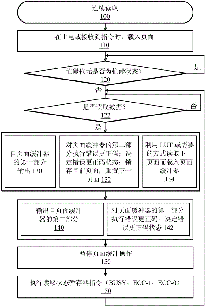
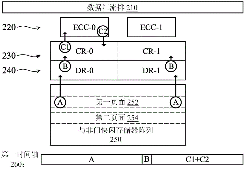
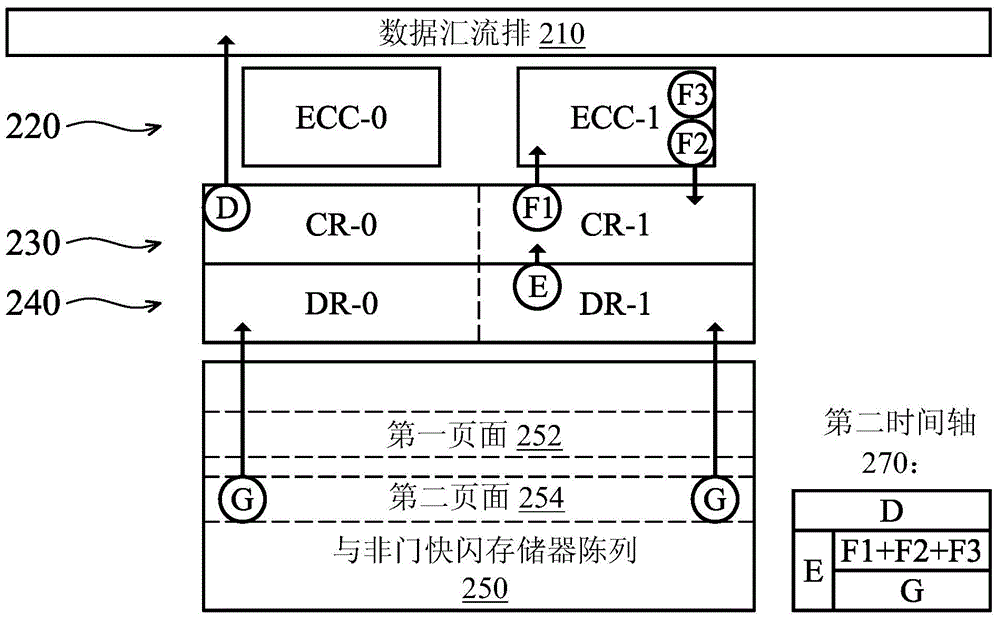
[0071] NAND memory devices can be fabricated with many characteristics compatible with NOR memory devices, including (1) multiple input / output (I / O) serial peripheral interface (SPI) / quick path interconnect (QPI) interfaces; (2) Package type with less number of pins (8*6mm with a density of 256Mb or higher), for example, WSON with 8 contacts, SOIC with 16 pins and BGA type package with 24 balls, with the use of The flexibility of large packages (such as VBGA-63 commonly used in general parallel or general serial NAND flash memory); (3) high clock frequency operation (such as 104MHz) versus high transfer rate (such as 50MHz / second); ( 4) Continuous reads across page boundaries with error correction code processing for fast code-mapping applications without latency; Bad block management (bad block management), logically continuous marked memory; and (6) through the value set by the user or the manufacturer, to determine the output start address is logic 0 or the user in the memo...


PUM


Abstract

The invention provides a memory reading method and a digital memory device. The digital memory device is divided into a data temporary memory and a data buffer of a cache register, an internal error correction code relative to the cache register and set by a user, and a rapid bad block management. When data reading is carried out, the internal error correction code is displayed by an error correction code status bit. The status (1:1) can represent that the output data of the whole multi-page includes a continuous read-out mode of more than 4 bit errors on each page, the state of the error correction code of each page or each page partition are required to be known, for the former, when the output page is finished, the state of the error correction code of the whole page is determined, and is stored in a state buffer; for the latter, before the corresponding page partition is output, the state of the error correction code of each page partition is determined and output. The error correction code treatment is integrated, and waiting time is not required.

Description

technical field [0001] The present invention relates to digital memory devices and methods of operation thereof, and more particularly to NAND flash memory with integrated error correction code processing and methods of operation thereof. Background technique [0002] NAND flash memory is quite popular in data storage, because the memory cell size of single-level (single level cell, SLC) NAND flash memory is inherently small, making single-level NAND above 512Mb Gate flash memory has a considerable advantage in cost versus density. [0003] NAND flash memory has also become quite popular for a variety of applications other than data storage, including code shadowing. Although commonly used single-level NAND flash memory has architectural, performance, data integrity, and damage area limitations that make it difficult to support high-speed code mapping applications suitable for serial NOR flash memory, various Technology has been developed to make NAND flash memory suitable...

Claims


Application Information

Patent Timeline
Patent Type & Authority Applications(China)
IPC IPC(8): G11C16/26G11C29/42
Inventor 欧伦·麦克
Owner WINBOND ELECTRONICS CORP
Why Eureka
Try Eureka