Transistor

A transistor and integrated technology, applied in the direction of transistors, electric solid-state devices, semiconductor devices, etc., can solve the problems of low breakdown voltage and achieve the effects of improving breakdown voltage, reducing trap effect, and weakening degree of bending

Inactive Publication Date: 2016-08-03
CHINA COMM TECH CO LTD +1
View PDF6 Cites 9 Cited by
  • Summary
  • Abstract
  • Description
  • Claims
  • Application Information

AI Technical Summary

Problems solved by technology

[0004] Based on this, it is necessary to provide a transistor for the low breakdown voltage of the existing high electron mobility transistor

Method used


Image

  • Transistor
  • Transistor
  • Transistor

Examples


Embodiment Construction

[0033] In order to make the object, technical solution and advantages of the present invention clearer, the present invention will be further described in detail below in conjunction with the accompanying drawings and embodiments. It should be understood that the specific embodiments described here are only used to explain the present invention, and do not limit the protection scope of the present invention.

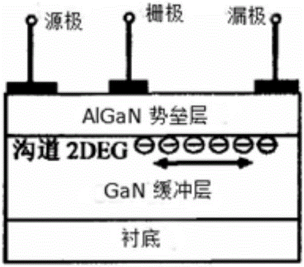
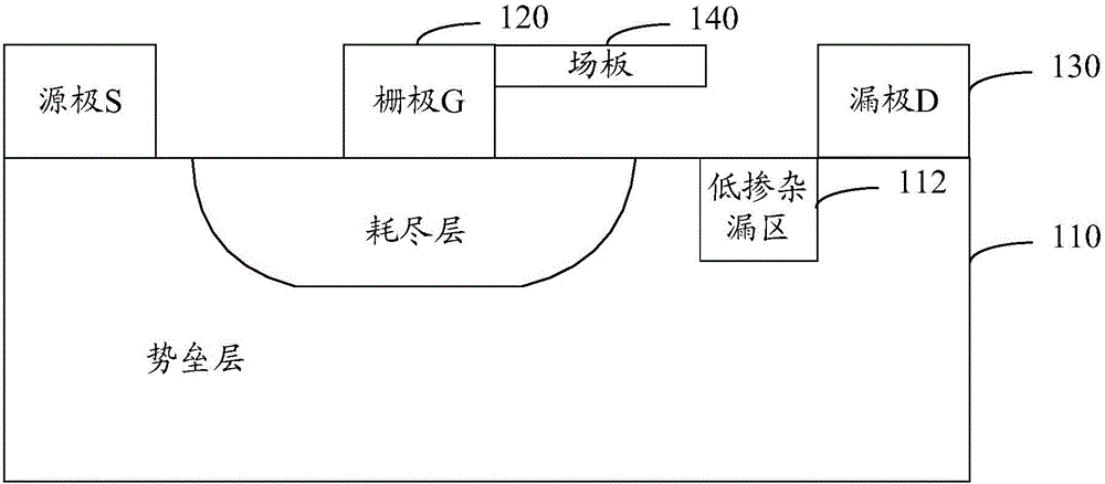
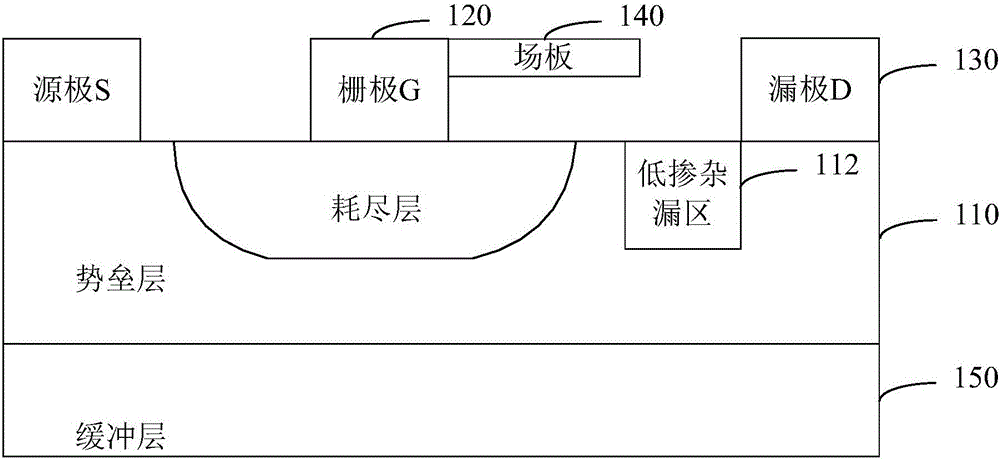
[0034] see figure 2 Shown is an embodiment of the transistor of the present invention. The transistor in this embodiment includes a barrier layer 110, a gate 120, a drain 130, a field plate 140, and a low-doped drain region 112;

[0035] The low-doped drain region 112 is arranged inside the barrier layer between the gate 120 and the drain 130, and one end of the low-doped drain region 112 coincides with the edge of the drain 130, and the other end of the low-doped drain region 112 coincides with the edge of the drain 130. The edges of the grid 120 do not coincide;

...


PUM


Abstract

The invention relates to a transistor. A lowly-doped drain region is arranged in a barrier layer of the transistor. Due to the difference in electronegativity between the lowly-doped drain region and the region in the barrier layer except the lowly-doped drain region, the lowly-doped drain region can help adjust the two-dimensional electron gas in the barrier layer, change the electric field intensity of a depletion layer under a gate in the barrier layer, make the electric field re-distributed, reduce the peak of the electric field, reduce the trap effect, and improve the breakdown voltage. Meanwhile, a field plate is introduced, the bending degree of the boundary of the depletion layer at the edge of the gate is reduced, electric field distribution is modulated, the peak of the electric field is reduced, the trap effect is reduced, and the breakdown voltage is further improved. Under the joint action of the lowly-doped drain region and the field plate, the breakdown voltage of the transistor is improved greatly, and the working stability of the transistor is increased.

Description

technical field [0001] The invention relates to the technical field of electronic devices, in particular to transistors. Background technique [0002] GaN material has a wide band gap, extremely high breakdown electric field, high thermal conductivity, radiation resistance, corrosion resistance and other good electrical properties. It is the second generation of compound semiconductor materials following the first generation of semiconductor materials Ge and Si. A typical representative of the third-generation semiconductor materials after GaAs and InP, it is an ideal material for making high-frequency, high-temperature, high-voltage, high-power electronic devices and high-power optoelectronic devices. More importantly, GaN materials can form an AlGaN / GaN structure, and under the action of spontaneous polarization and piezoelectric polarization, a two-dimensional electron gas (two-dimensional electron gas, 2DEG) with a higher concentration than the second-generation compound...

Claims


Application Information

Patent Timeline
Patent Type & Authority Applications(China)
IPC IPC(8): H01L29/778
CPCH01L29/788H01L29/778H01L2924/13064
Inventor 王佳佳丁庆
Owner CHINA COMM TECH CO LTD
Why Eureka
Try Eureka