FPGA circuit transmission delay rest system and method based on TDC

A transmission delay and testing system technology, applied in electronic circuit testing, measuring electricity, measuring devices, etc., can solve the problems of strong professional and technical requirements of testers, difficulty in testing internal modules of chips, and high testing costs, reducing equipment and manpower. Low cost, low test equipment requirements, good versatility

Inactive Publication Date: 2016-08-10
FUDAN UNIV
View PDF4 Cites 14 Cited by
  • Summary
  • Abstract
  • Description
  • Claims
  • Application Information

AI Technical Summary

Problems solved by technology

This approach faces problems such as high testing costs, strong requirements for the professional skills of testers, and off-chip interference.
And ATE equipment can only be tested off-chip through I / O pins, it is difficult to test the internal modules of the chip

Method used


Image

  • FPGA circuit transmission delay rest system and method based on TDC
  • FPGA circuit transmission delay rest system and method based on TDC
  • FPGA circuit transmission delay rest system and method based on TDC

Examples


Embodiment Construction

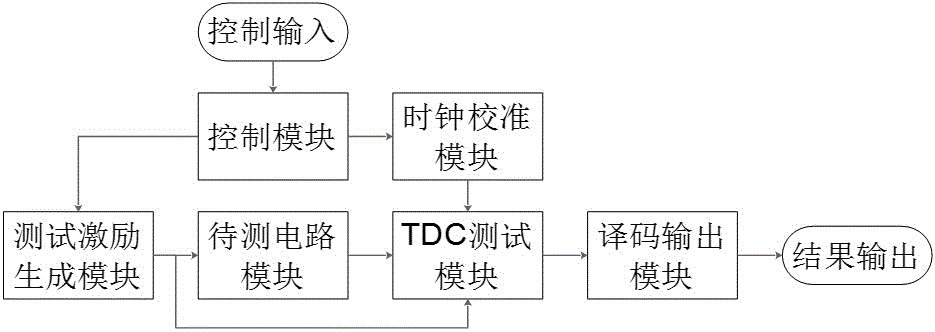
[0019] The basic implementation process of the system of the present invention is as follows: figure 2 shown.

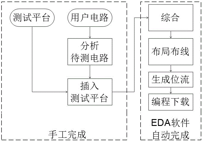
[0020] Among them, the EDA tool generally chooses the EDA tool provided by the FPGA chip manufacturer itself, such as the ISE series software of Xilinx Company, or the Quartus series software of Altera Company. The test platform is generally described in the form of industry-standard HDL code, and an appropriate TDC structure is selected according to the characteristics of the FPGA to be tested. The circuit to be tested can flexibly choose methods such as hard macro (hard macro), IP core, HDL code description according to the test requirements, as long as it can accept EDA tool synthesis.

[0021] Taking a test process based on ISE EDA software as an example, the TDC test platform is described in the form of HDL language, and the circuit to be tested is described in the form of hard macros to avoid comprehensive interference. Before starting the test, first creat...


PUM


Abstract

The invention belongs to the integrated circuit technical filed, and concretely discloses an FPGA (Field Programmable Gate Array) circuit transmission delay test system and method based on a TDC (time-digital converter) method. The test system comprises: a circuit module to be tested, a test excitation generation module, a TDC module, a decoding output module, a time calibration module and a control module. The system can utilize a TDC method to count delay chains, test transmission delay of an FPGA internal circuit more conveniently, and utilize internal resources in an FPGA chip to construct BIST (Build-in Self Test) for test, has the characteristics of low test cost, sound anti-interference performance, great transportability, independence of test tools, etc., and has great application values on test various transmission delay parameters in an FPGA including switch parameters, interconnection delay, combinational logic delay and CLK-Q delay of a configurable logic block (CLB), a programmable input output box (IOB), a block random access memory (BRAM), a digital signal processor (DSP) and a programmable interconnection FPGA combination module circuit.

Description

technical field [0001] The invention belongs to the technical field of integrated circuits, and in particular relates to a system and a method for testing signal transmission delays of various circuits in an FPGA circuit chip. Background technique [0002] Field Programmable Gate Array (Field Programmable Gate Array, FPGA) is a semi-custom circuit developed on the basis of PAL, GAL, CPLD and other programmable devices. After the chip is manufactured, it can also change the function according to the user's needs through programming, and can be repeatedly erased and modified, so that no additional changes to the hardware design are required when the system is debugged and upgraded, which greatly improves design flexibility, shortens the design cycle, and reduces design cost. Modern FPGAs are characterized by the integration of block memory (BRAM), digital signal processing, and Device (DSP: Digital Signal Processing), clock manager (CM: clock managers) and other resources. ...

Claims


Application Information

Patent Timeline
IPC IPC(8): G01R31/28
CPCG01R31/2856
Inventor 来金梅石超王健
Owner FUDAN UNIV
Why Eureka
Try Eureka