Method of processing a target object
A technology of processed objects and processing methods, applied in semiconductor/solid-state device manufacturing, electrical components, circuits, etc., can solve problems such as the influence of resolution limits, and achieve the effect of reducing the deviation of film thickness
- Summary
- Abstract
- Description
- Claims
- Application Information
AI Technical Summary
Problems solved by technology
Method used
Image

Examples
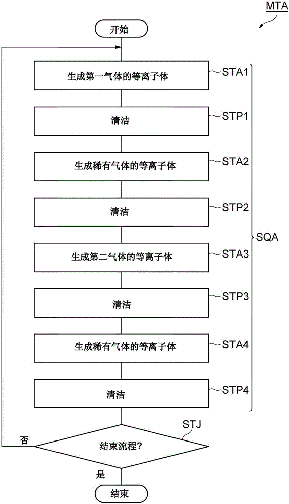
experiment example 1~2 and comparative experiment example 1
[0123] In Experimental Example 1, a silicon oxide film was formed on the flat surface of a wafer having a diameter of 300 mm by the method MTA. In addition, in Experimental Example 2, a silicon oxide film was formed on the flat surface of a wafer with a diameter of 300 mm by the method MTB. Also, in Comparative Experiment 1, a silicon oxide film was formed on the flat surface of a wafer with a diameter of 300 mm by omitting Step STA2 , Step STP2 , Step STA4 , and Step STP4 from the method MTA.
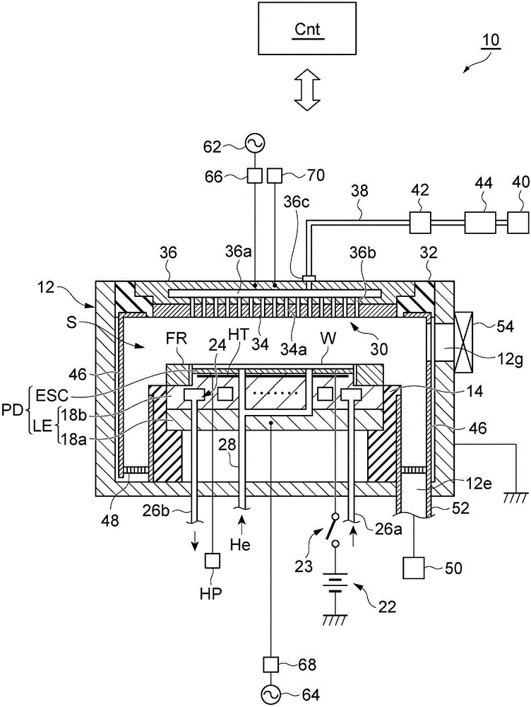
[0124] In Experimental Example 1, the conditions of each step were set to the conditions shown below. In addition, the number of executions of the flow SQA in Experimental Example 1 is 60 times.
[0125]
[0126] ·Pressure inside the processing container: 200mTorr (26.66Pa)
[0127] ·SiCl 4 Gas flow: 14sccm
[0128] ·Ar gas flow rate: 200sccm
[0129] · High-frequency power of the first high-frequency power supply 62 (supplied to the upper electrode 30 ): 60 MHz, 100 W
[0130]...
experiment example 3 and comparative experiment example 2
[0195] In Experimental Example 3, a silicon oxide film was formed on the flat surface of a wafer with a diameter of 300 mm by the method MTA. Also, in Comparative Experiment Example 2, a silicon oxide film was formed on the flat surface of a wafer with a diameter of 300 mm by omitting Step STP1, Step STP2, Step STP3, and Step STP4 from the method MTA.
[0196] In Experimental Example 3, the conditions of each step were set to the conditions shown below. In addition, the number of executions of the flow SQA in Experimental Example 3 is 60 times.
[0197]
[0198] ·Pressure inside the processing container: 200mTorr (26.66Pa)
[0199] ·SiCl 4 Gas flow: 14sccm
[0200] ·Ar gas flow rate: 200sccm
[0201] · High-frequency power of the first high-frequency power supply 62 (supplied to the upper electrode 30 ): 60 MHz, 100 W
[0202] · High-frequency bias power of the second high-frequency power supply 64: 13.56 MHz, 0 W
[0203] · Processing time: 2 seconds
[0204]
[02...
experiment example 4~6 and comparative experiment example 3
[0240] In Experimental Example 4, a silicon oxide film was formed on the flat surface of a wafer with a diameter of 300 mm by the method MTA. In Experimental Example 5 and Experimental Example 6, a silicon oxide film was formed on the flat surface of a wafer having a diameter of 300 mm by the method MTB. However, in Step STB4 of Experimental Example 5, the flow rate of Ar gas was set to 200 sccm, and in Step STB4 of Experimental Example 6, the flow rate of Ar gas was set to 1300 sccm. In Comparative Experiment Example 3, a silicon oxide film was formed on the flat surface of a wafer having a diameter of 300 mm by omitting Step STA2 and Step STA4 from the method MTA. In addition, in Experimental Examples 4 to 6 and Comparative Experimental Example 3, the conditions of each step were set such that the film thicknesses of the silicon oxide films were substantially equal.
[0241] Specifically, in Experimental Example 4, the conditions of each step were set to the conditions show...
PUM
 Abstract
Description
Claims
Application Information
 - R&D
- Intellectual Property
- Life Sciences
- Materials
- Tech Scout
- Unparalleled Data Quality
- Higher Quality Content
- 60% Fewer Hallucinations
Browse by: Latest US Patents, China's latest patents, Technical Efficacy Thesaurus, Application Domain, Technology Topic, Popular Technical Reports.
© 2025 PatSnap. All rights reserved.Legal|Privacy policy|Modern Slavery Act Transparency Statement|Sitemap|About US| Contact US: help@patsnap.com