RTD with InGaN sub quantum well with gradually changing In component

A quantum well and diode technology, applied in the field of electronics, can solve problems such as low mobility, low two-dimensional electron gas concentration, operating frequency and output power that cannot meet the output requirements of terahertz devices, etc., to overcome large and small leakage currents. Effect of leakage current, high peak current

Active Publication Date: 2016-08-10
XIDIAN UNIV
View PDF5 Cites 10 Cited by
  • Summary
  • Abstract
  • Description
  • Claims
  • Application Information

AI Technical Summary

Problems solved by technology

The disadvantage of this method is that because the two-dimensional electron gas concentration at the AlAs / InGaAs interface is not high and the mobility is not high, the operating frequency and output power cannot meet the output requirements of terahertz devices.

Method used


Image

  • RTD with InGaN sub quantum well with gradually changing In component
  • RTD with InGaN sub quantum well with gradually changing In component
  • RTD with InGaN sub quantum well with gradually changing In component

Examples


Embodiment 1

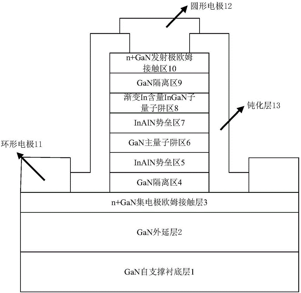
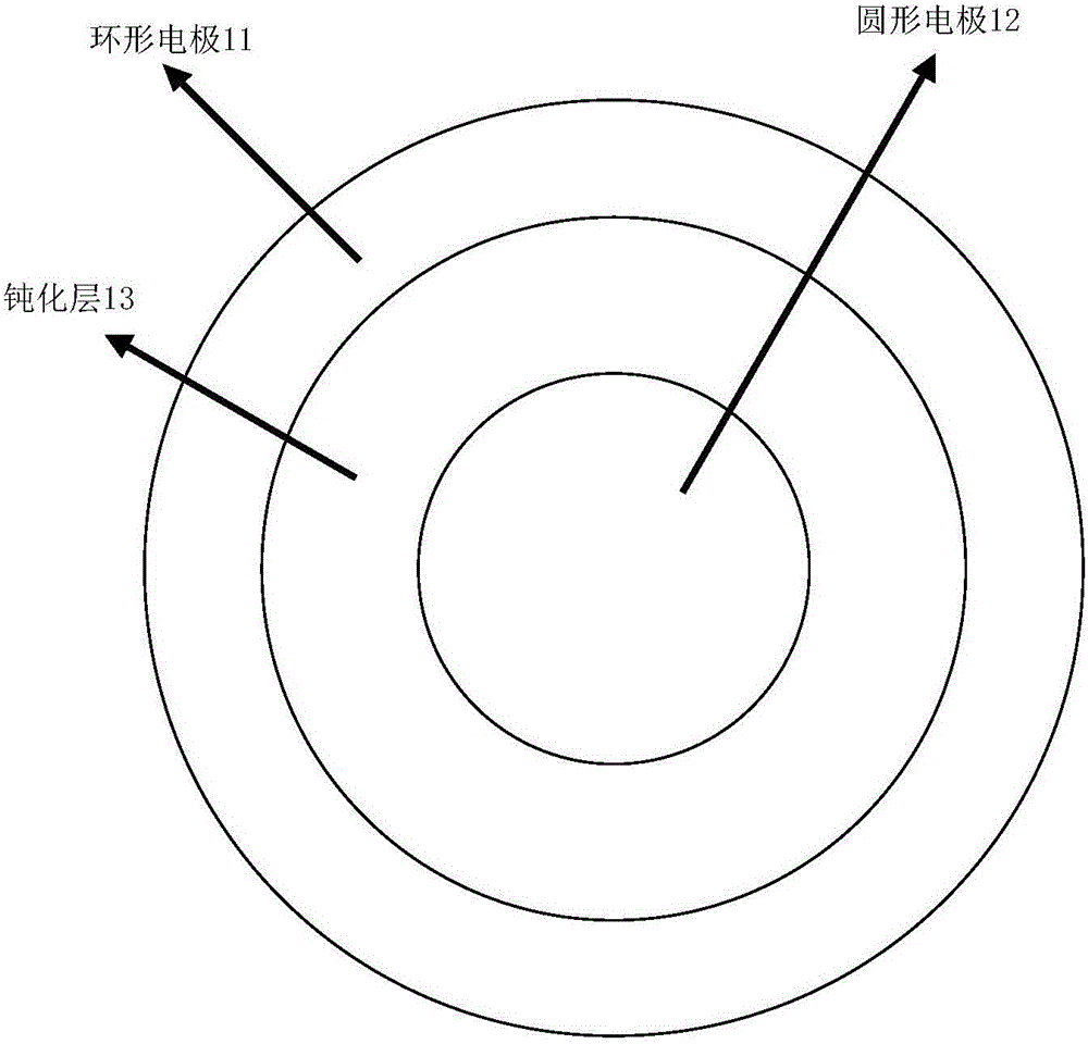
[0139] Embodiment 1: The In composition of making the first layer InGaN sub-quantum well is 3%, the In composition of the second layer InGaN sub-quantum well is 4%, and the In composition of the third layer InGaN sub-quantum well is 5%. Gradient In composition InGaN sub-quantum well layer.

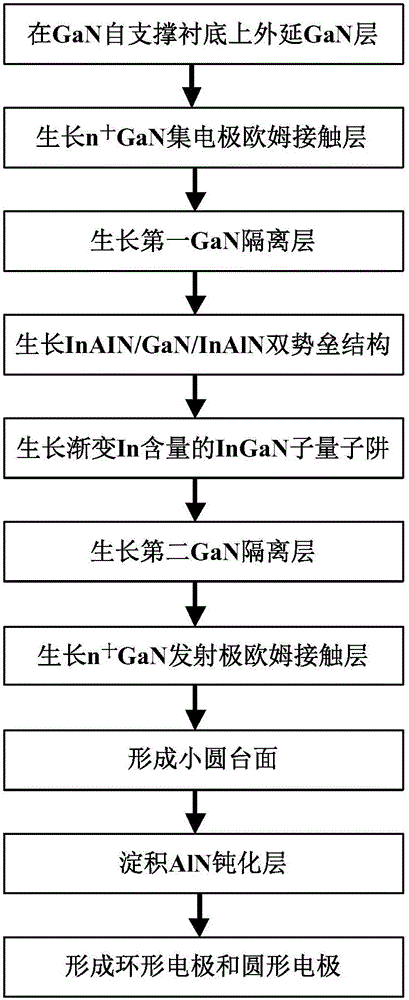
[0140] Step 1: Epitaxial GaN layer on GaN free-standing substrate.

[0141] A layer of GaN is epitaxially grown on the substrate by metal-organic chemical vapor deposition (MOCVD).

[0142] The specific steps of the metal organic chemical vapor deposition MOCVD method are as follows.

[0143] Prepare the source, use triethylgallium as the gallium source, and high-purity nitrogen as the nitrogen source.

[0144] The gas in the reaction chamber is pumped out, and the substrate is sent into the reaction chamber.

[0145] The temperature in the reaction chamber was raised to a growth temperature of 450° C., and the pressure was 40 Torr.

[0146] After the temperature is reached, the galliu...

Embodiment 2

[0235] Embodiment 2: The In composition of making the first layer InGaN sub-quantum well is 4%, the In composition of the second layer InGaN sub-quantum well is 5%, and the In composition of the third layer InGaN sub-quantum well is 6%. Gradient In composition InGaN sub-quantum well layer.

[0236] Step A: Epitaxial GaN layer on GaN free-standing substrate.

[0237] A layer of GaN is epitaxially grown on the substrate by metal-organic chemical vapor deposition (MOCVD).

[0238] The specific steps of the metal organic chemical vapor deposition MOCVD method are as follows.

[0239] Prepare the source, use triethylgallium as the gallium source, and high-purity nitrogen as the nitrogen source.

[0240] The gas in the reaction chamber is pumped out, and the substrate is sent into the reaction chamber.

[0241] The temperature in the reaction chamber was raised to a growth temperature of 450° C., and the pressure was 40 Torr.

[0242] After the temperature is reached, the gallium ...

Embodiment 3

[0331] Embodiment 3: The In composition of making the first layer InGaN sub-quantum well is 5%, the In composition of the second layer InGaN sub-quantum well is 6%, and the In composition of the third layer InGaN sub-quantum well is 7%. Gradient In composition InGaN sub-quantum well layer.

[0332] Step 1: Epitaxial GaN layer on GaN free-standing substrate.

[0333] A layer of GaN is epitaxially grown on the substrate by metal-organic chemical vapor deposition (MOCVD).

[0334] The specific steps of the metal organic chemical vapor deposition MOCVD method are as follows.

[0335] Prepare the source, use triethylgallium as the gallium source, and high-purity nitrogen as the nitrogen source.

[0336] The gas in the reaction chamber is pumped out, and the substrate is sent into the reaction chamber.

[0337] The temperature in the reaction chamber was raised to a growth temperature of 450° C., and the pressure was 40 Torr.

[0338] After the temperature is reached, the galliu...


PUM


Abstract

The invention discloses an RTD with an InGaN sub quantum well with a gradually changing In content. The RTD comprises a GaN epitaxial layer, an n+GaN collector electrode ohmic contact layer, a first GaN isolation layer, a first InAlN barrier layer, a GaN main quantum layer, a second InAlN barrier layer, an InGaN sub quantum well with a gradually changing In component, a second GaN isolation layer, an n+GaN emitter electrode ohmic contact layer and a circular electrode which are successively distributed on a substrate from bottom to top, an annular electrode which is disposed on the n+GaN collector electrode ohmic contact layer and is not in contact with the first GaN isolation layer, and an AlN passivation layer which is disposed on the n+GaN collector electrode ohmic contact layer. According to the invention, an InGaN sub quantum well with a gradually changing In component and an AlN material passivation layer are introduced to the RTD, such that peak currents are increased, output power is improved, and device power consumption is reduced.

Description

technical field [0001] The invention belongs to the field of electronic technology, and further relates to a resonant tunneling diode (Resonant Tunneling Diode, RTD) of a wide bandgap semiconductor GaN material of a graded indium-In composition indium-gallium-nitride InGaN sub-quantum well in the field of microelectronic device technology. The invention can be used as a high-frequency and high-power device and applied in the fields of microwave and high-speed digital circuits. Background technique [0002] Resonant tunneling diode (RTD) is a new type of nano-device that works by quantum resonant tunneling effect. It has bistable, self-locking characteristics and obvious negative resistance characteristics. RTDs have very low intrinsic capacitance, so they have high speeds and operating frequencies. Compared with other nano-devices, its development is faster and more mature, and it has entered the application stage. With the continuous development of device design and techn...

Claims


Application Information

Patent Timeline
Patent Type & Authority Applications(China)
IPC IPC(8): H01L29/15H01L29/20H01L21/329H01L29/88
CPCH01L29/151H01L29/2003H01L29/66219H01L29/882
Inventor 张进成黄金金于婷陆芹郝跃薛军帅杨林安林志宇
Owner XIDIAN UNIV
Why Eureka
Try Eureka